How to use ADC in AVR
This is the 5th tutorial in the AVR series and today we will cover the ADC peripheral. In the previous tutorial we saw how to send the data to the serial terminal by using the UART. We will use the information from the previous tutorial and send the ADC value to the serial monitor.
In today’s tutorial, we will read the ADC in a simplest possible way. we will use the blocking mode where the application will wait for the conversion to finish. Also we will trigger the conversion manually even though the AVR controllers do support Auto tigger modes. Basically we will cover the simplest method today and the more complicated methods will be covered in the future tutorials.
The ATTiny85 features a 10 bit ADC, which is connected to a 4-channel Analog Multiplexer which allows one differential voltage input and four single-ended voltage inputs constructed from the pins of Port B. The minimum value from the ADC represents GND and the maximum value represents the voltage on VCC, the voltage on the AREF pin or an internal 1.1V / 2.56V voltage reference. The voltage reference for the ADC may be selected by using the Registers provided of the ADC.
Connection
Below is the image showing the connection between the MCU and the Potentiometer.
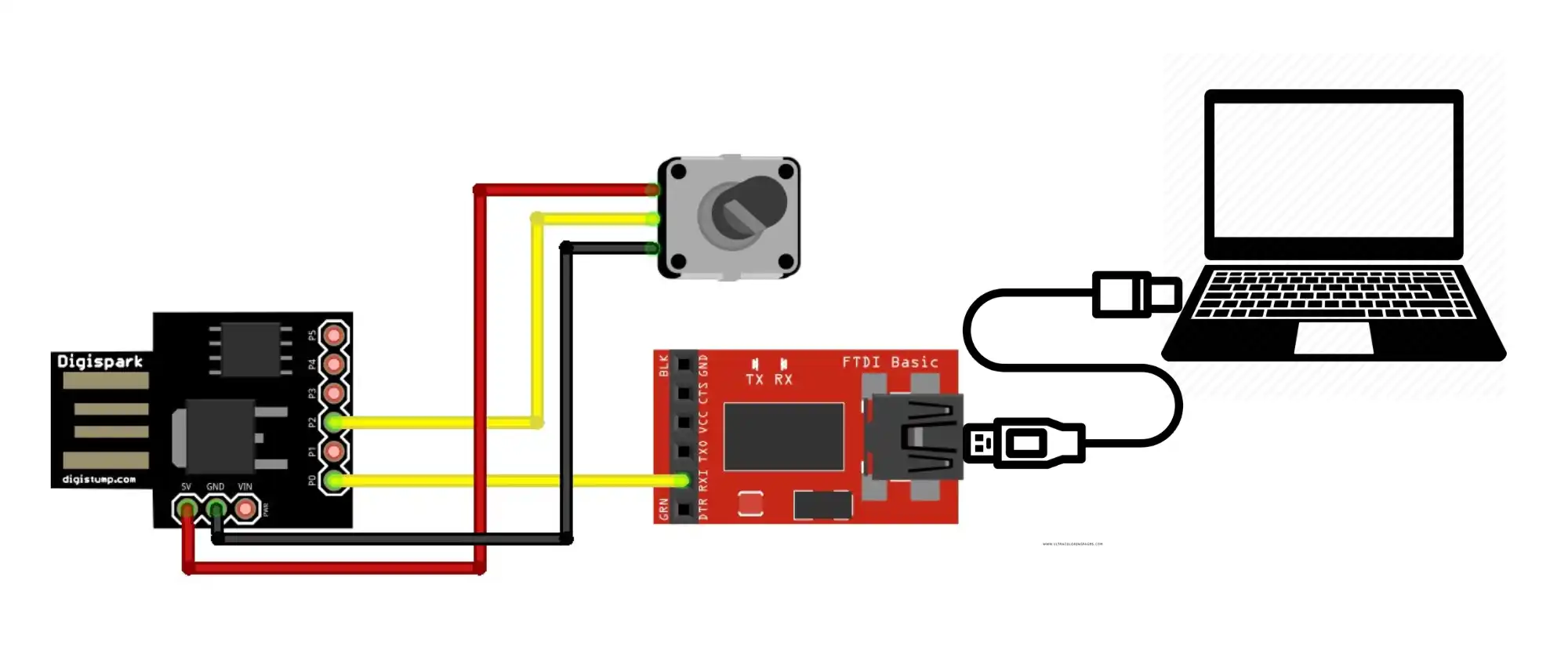
- As shown in the image above, the potentiometer is powered by the MCU itself. The 2 end pins are provided with 5V and Gnd.
- The middle pin of the potentiometer is connected to the pin PB2. This is where the voltage will be read and converted to the digital value.
- The pin PB0 is connected to the RX pin of the FT232 USB to UART converter. This pin will be used to send the data to the serial monitor using the UART.
Some insight into the Code
We will first see the initialisation of the ADC. Then cover how to read and arrange the ADC value. Finally we will implement everything in the main function.
Let’s start with the initialisation.
ADC Initialisation
void ADC_init (void)
{
ADMUX Register
The first Register in the datasheet is the ADMUX Register. It is responsible for selecting the multiplexer and the reference voltage.
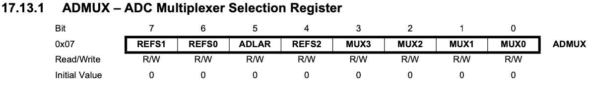
The Bits3:0 (MUX3 to MUX0) are used to select the respective ADC input. In today’s tutorial we will cover the single ended mode, so we will just focus on the selection of the single ended ADC inputs.
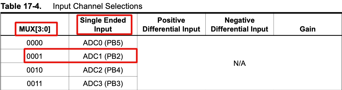
I am going to use the ADC1. The ADC input pin will be the pin PB2. To select ADC1 the MUX[3:0] must be configured as 0001, which means the MUX0 should be set HIGH.
The Bits 7, 6 and 4 can be used to select the voltage reference for the ADC. The minimum voltage for the ADC is GND and the maximum voltage can be wither the VCC, the voltage on the AREF pin or an internal 1.1V / 2.56V voltage reference. This selection can be made by using the bits REFS2, REFS1 and REFS0.
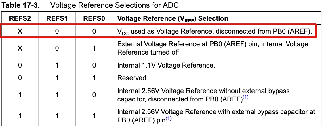
As shown in the picture above, different combination of the bits results in different reference voltage for the ADC. I am going to use the Vcc (5V) as the reference as I have connected the potentiometer to the Vcc of the board itself.
Note that the AREF (Analog Reference) is being used at the pin PB0. This is where you can connect the external reference voltage. The pin PB0 is also used for sending the data via the UART. SO if you do use the AREF, change the UART pin to something else.
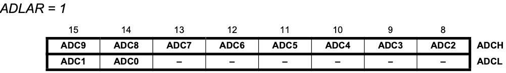
The Bit5 (ADLAR) is used to adjust the presentation of the ADC conversion result in the ADC Data Register. The data register is only 8 bit wide, whereas the ADC has the resolution of 10 bits. This is why the data stored in the data register in the 2 byte format. The ADLAR bit decides how this data will be stored.
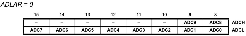
I am keeping this bit 0, so that we get the output as shown in the first image.
The combined data to be written in the ADMUX register is shown below.
ADMUX = 1<<MUX0; // ADC1 with PB2, Vcc as referenceWe only need to write a 1 to the MUX0 bit and the rest of the bits should be kept 0.
ADCSRA Register
The ADCSRA (Status and Control Register A) is used to enable/disable the ADC, Set different trigger modes, and to set the prescaler for the ADC.
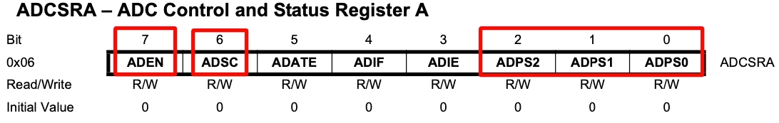
- ADEN is used to enable/disable the ADC.
- ADSC is used to start the conversion.
- ADATE is used to select the auto trigger mode for the ADC.
- ADIE is used to enable the interrupt.
- ADIF is the interrupt flag and is set when the ADC conversion is complete.
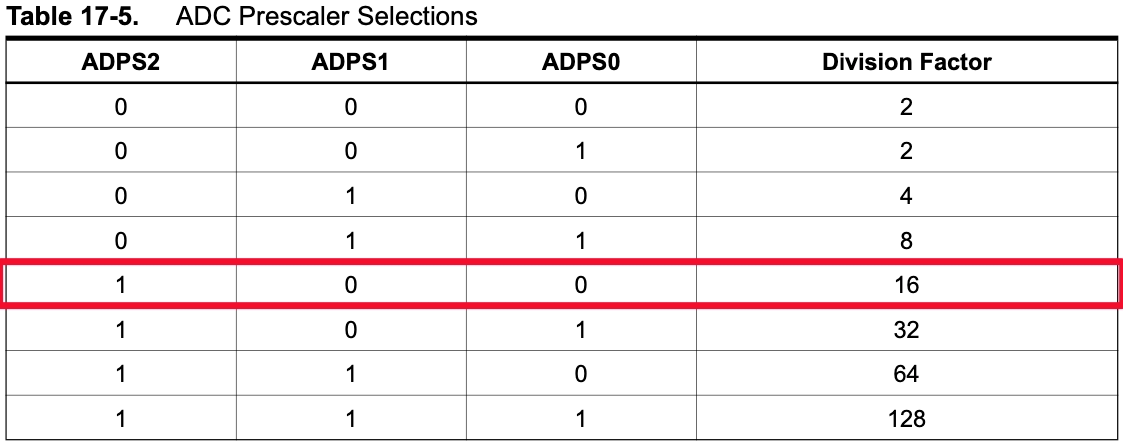
- ADPS2:ADPS0 are used to set the prescaler for the ADC.
Since we are only covering the simpler implementation of the ADC, we will only focus on the bits 7, 6 and 2:0. The auto trigger mode and the interrupt will be covered later in the future tutorials.
Using potentiometer does not require the clock precision. I am just using a random prescaler value.
   ADCSRA = (1<<ADEN)|(1<<ADPS2); // enable ADC, PSC = 16, ADC CLK = 1000000/16
}
ADC Convert
To Read the ADC value, we will start the conversion. When the conversion is finished, we will read the ADC data registers and combine the 2 bytes into a single 16 bit value.
uint16_t ADC_Convert (void)
{
	ADCSRA |= 1<<ADSC;  // start conversion
	while ((ADCSRA&(1<<ADSC)) == 1){}  // wait for the conversion to finish
	uint8_t adcl = ADCL; // read ADCL register
	uint8_t adch = ADCH; // read ADCH Register
	uint16_t val = ((adch<<8)|adcl)&0x3FF;  // combine into single 10 bit value, 0x3FF-> 0b11 1111 1111
	return val;
}- We will start the conversion by writing a 1 to the ADSC bit in the Status and Control Register A.
- This bit remain high as long as the conversion is going on. So we will wait for the bit to go low.
- The read the ADCL and ADCH data registers and store them in separate bytes.
- Combine the 2 bytes into a single 16 bit value and mask it with the 0x3FF to convert it to 10 bit value.
- Finally return the value.
The main function
uint16_t ADC_VAl = 0;
char ADC_VAL_Char[5];

int main(void)
{
    uart_init();
    ADC_init();
    while(1)
    {
    	ADC_VAl = ADC_Convert();
	sprintf(ADC_VAL_Char, "%u\n", ADC_VAl);
	uart_str(ADC_VAL_Char);
	_delay_ms(200);
    }
}- In the main function we will initialise the UART and the ADC peripherals.
- In the while loop Read the ADC value and store it in the 16 bit variable.
- The the sprints function will convert the converted value in the character format.
- Finally we will send the character array to the UART.
- The loop will run every 200ms.
Result
Below is the GIF showing the output on the serial console.
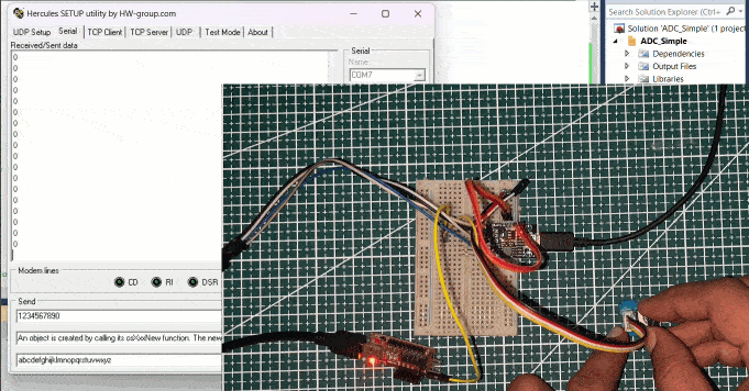
You can see the rotation of potentiometer increases the value from 0 to 1023. This is the highest achievable value in case of the 10 bit resolution.
The value 0 indicate the Voltage on the pin PB2 is 0 and the value 1023 represents the voltage is same as Vcc.