
Home ▸ STM32 Tutorials ▸
Updated On: March 23, 2026
QUADSPI Write, Read, Memory Mapped mode
This is the 7th tutorial in the W25Q Flash series, and today we will see how to use the W25Q flash memory with the QuadSPI peripheral in STM32. In this tutorial we will see the connection in the QuadSPI mode, and how to Write and Read data from the memory. We will also see how to use the memory mapped mode so the MCU can see the external flash memory as the internal flash.
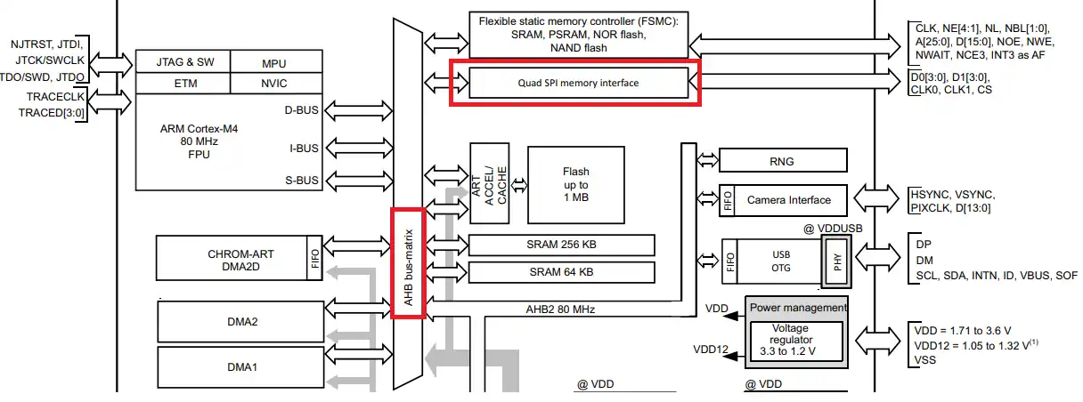
I am using the W25Q32JVSSIQ nor flash memory from winbond, and STM32L496-P nucleo board from ST. The board supports the QSPI peripheral with quad lines. The maximum speed in the SDR (Single data Rate) mode can go up to 60MHz, and the maximum memory size in the memory mapped mode can be upto 256 MBytes.
VIDEO TUTORIAL
You can check the video to see the complete explanation and working of this project.
Connection
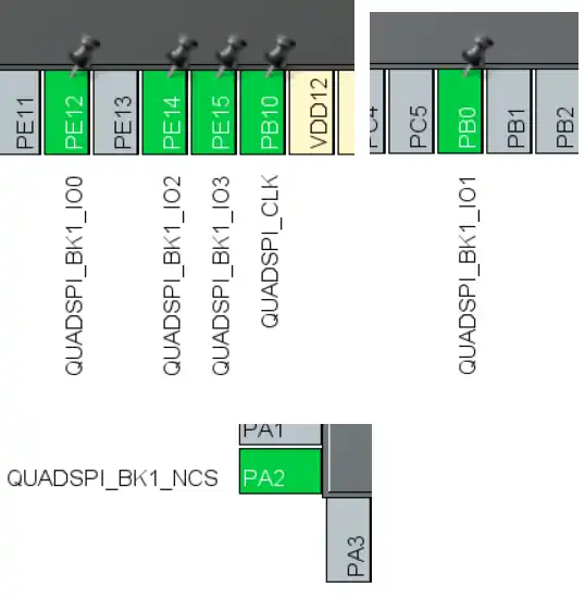
The QuadSPI uses 4 data lines to communicate to the device. Below is the image showing the connection between the W25Q32 and the STM32L496.
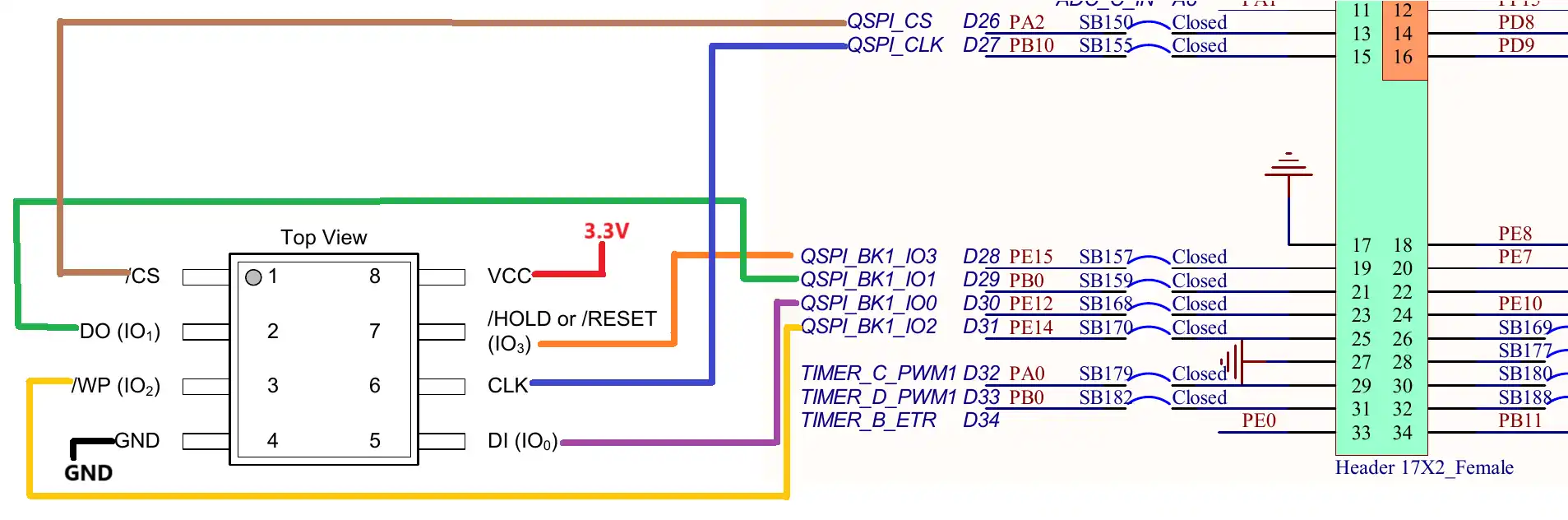
The memory chip is powered with 3.3V and the other pins are connected to their respective counterpart in the MCU.
CubeMX Setup
I have configured the clock at the maximum 80MHz frequency. This sets the AHB bus at the same clock.
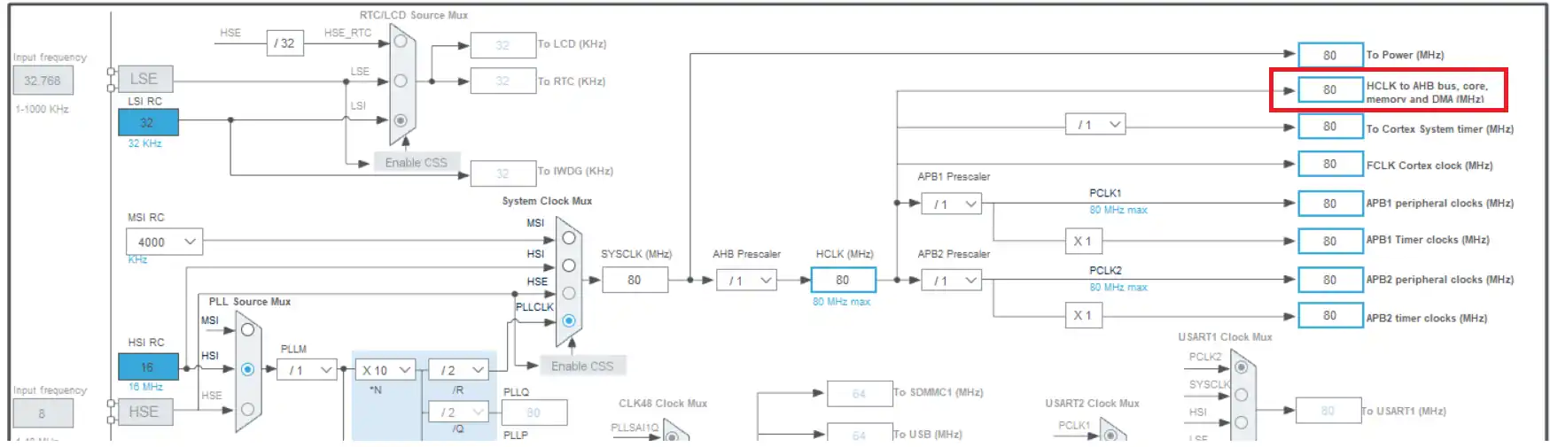
As per the datasheet of the STM32L496, the QSPI is clocked by the AHB bus.
Since the AHB clock is at 80 MHz, the QSPI clock is also at the same frequency. But as I mentioned in the beginning, the board supports a maximum of 60MHz QSPI speed, we need to reduce the clock using prescaler.
Below is the configuration for the WSPI parameters.
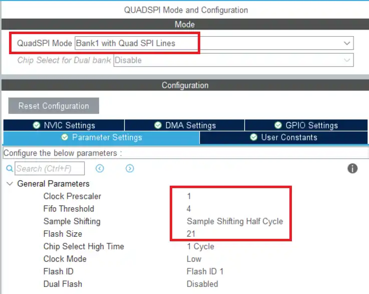
- The Prescaler of 1 (actually the value 2) will reduce the QSPI clock to 40MHz. (80MHz/2)
- Set the fifo threshold to 4, and the sample shifting to half cycle.
The flash size is based on the size of the external flash you are using. It can be calculated using the formula below.
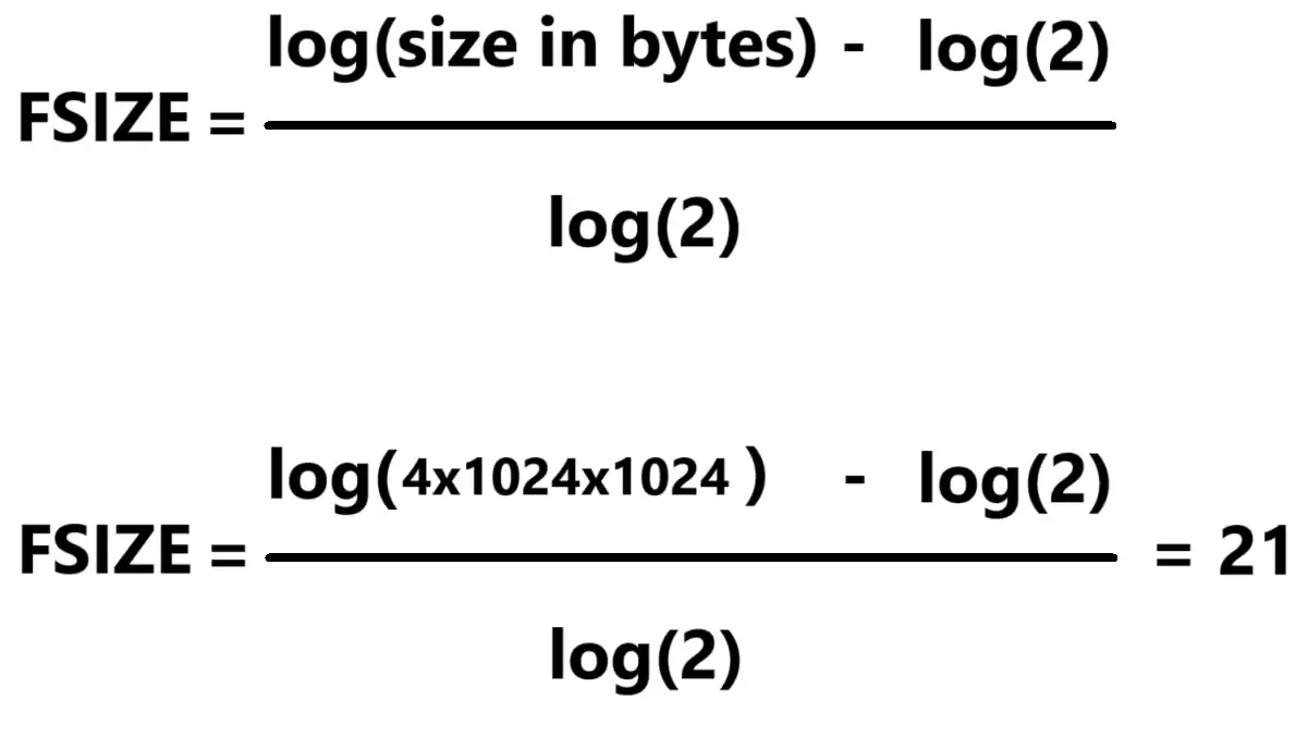
I have the W25Q32JV, which is 4MB in size. As per the calculation, the Flash size is 21.
The pins are configures as per the connection shown above.
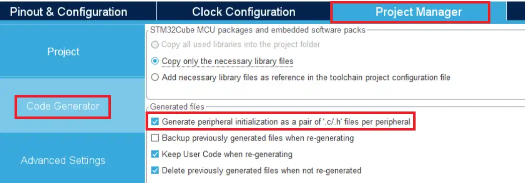
Also make sure to check the box shown below to generate the separate files for the peripherals.
The code
I have modified the ST’s quadSPI library files so that they can be used with the W25Q series nor flash memories. You can get the files by downloading the project at the end of this post.
You need to copy the code inside the /* USER CODE BEGIN 0 */ and /* USER CODE END 0 */ in the respective position in the quadspi.c file.
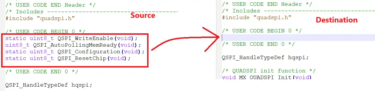
Similarly copy the code inside the /* USER CODE BEGIN 1 */ and /* USER CODE END 1 */ to the respective position.
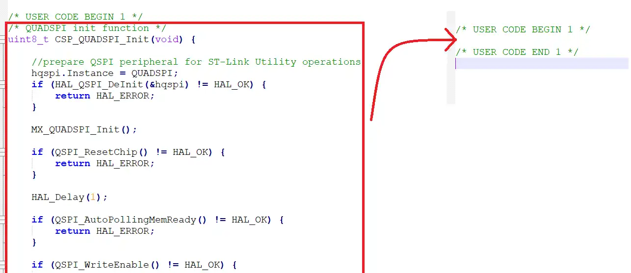
Also replace the content of the quadspi.h file.
If you are using any other memory type than the W25Q32, you need to change the MEMORY FLASH SIZE parameter in the quadspi.h file.
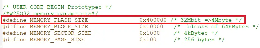
I have defined the MEMORY SIZE of 4MB for the W25Q32.
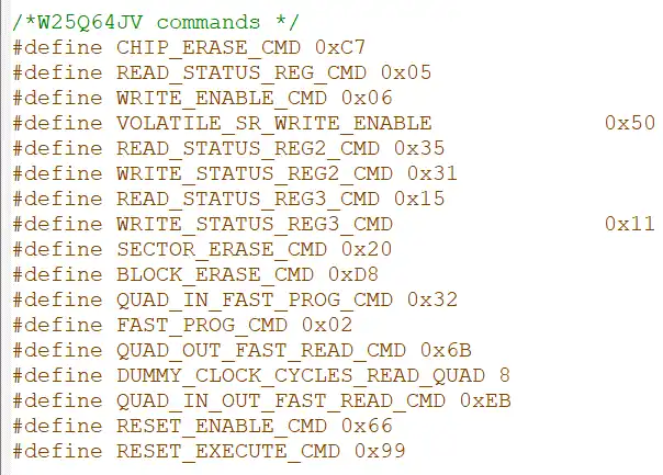
Also cross check the commands defined with the datasheet of the memory.
The main function
Inside the main function, we will perform the write and read operations. The code is shown below.
uint8_t writebuf[] = "Hello world from QSPI";
uint8_t Readbuf[100];

  if (CSP_QUADSPI_Init() != HAL_OK) Error_Handler();

  if (CSP_QSPI_Erase_Chip() != HAL_OK) Error_Handler();

  if (CSP_QSPI_WriteMemory(writebuf, 0, sizeof(writebuf)) != HAL_OK) Error_Handler();

if (CSP_QSPI_Read(Readbuf, 0, 100) != HAL_OK) Error_Handler();I have defined a write buffer which we will write to the memory, and a read buffer where the data read from the memory will be stored.
- Here we will first initialize the quadSPI.
- Then erase the entire chip. This operation may taker around 10 to 20 seconds.
- Now write the writebuf to the memory. The data will be written to the address 0, which is with respect to the memory. So basically at the start of the memory.
- Then we will read 100 bytes from the address 0, and store them in the Readbuf.
Result
Below is the image showing the result in the debugger.
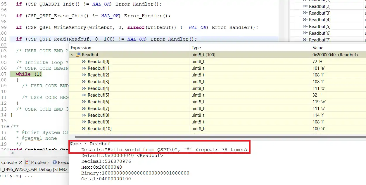
You can see that we received the same data what we wrote in the memory. The data is 22 bytes long and the rest of the bytes are 0xFF. This is because we erased the entire flash memory and hence it now have the data 0xFF.
You can check out the video towards the end of this post to see the detailed working.
Memory Mapped Mode
The Memory Mapped Mode can be used so that the MCU can see the external flash memory as the internal memory, basically a part of it. We will see how this works now.
Let’s enable the memory mapped mode and read the data from the memory.
  if (CSP_QUADSPI_Init() != HAL_OK) Error_Handler();

  if (CSP_QSPI_Erase_Chip() != HAL_OK) Error_Handler();

  if (CSP_QSPI_WriteMemory(writebuf, 0, sizeof(writebuf)) != HAL_OK) Error_Handler();

//  if (CSP_QSPI_Read(Readbuf, 0, 100) != HAL_OK) Error_Handler();

  if (CSP_QSPI_EnableMemoryMappedMode() != HAL_OK) Error_Handler();

memcpy(Readbuf, (uint8_t *) 0x90000000, sizeof(writebuf));- Here we will first initialize the quadSPI.
- Then erase the entire chip. This operation may taker around 10 to 20 seconds.
- Now write the writebuf to the memory. The data will be written to the address 0, which is with respect to the memory. So basically at the start of the memory.
- Then enable the memory mapped mode.
- And finally read the data from the address 0x90000000, and store it in the Readbuf.
Note that I am using the memcpy function to transfer the data from the location 0x90000000 to the Readbuf. The fact that we can use this function means that the MCU treats the memory at the address 0x9000000 as the internal memory.
The QSPI address for most of the MCUs is 0x90000000. But you should verify it with the reference manual of your controller once. Below is the image showing the memory map for the STM32L496 MCU.
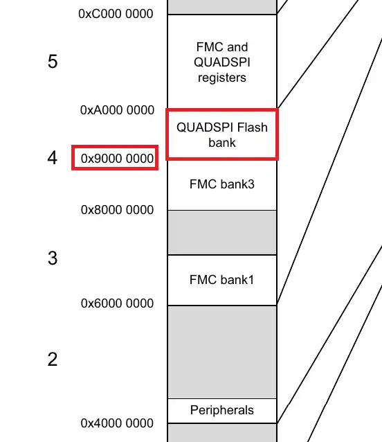
You can see the QUADSPI Flash bank is located at the address 0x90000000. Basically this space is reserved for the QuadSPI memory, and if we are using one, this is where we can access it.
Let’s see the output of the above code.
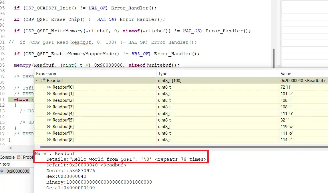
As you can see in the image above, the data in the Readbuf is same as what we stored in the memory. We were able to use the memcpy function so the MCU does see the external flash as a part of it.
We can confirm this by checking the memory viewer in the debugger.
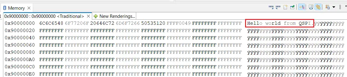
You can see the data in the memory viewer. This is only possible for the internal memories, and hence the memory mapped mode sets the external flash memory as the part of the MCU, so it can treat the memory as the internal one.
STM32 W25Q Flash Tutorials Series

W25Q Flash Series Part 2 – Read Data from Device
W25Q Flash Series Part 3 – How to Erase Sectors

W25Q Flash Series Part 4 – How to Program Pages
W25Q Flash Series Part 5 – how to update sectors

W25Q Flash Series Part 6 – Integers floats and 32bit Data

W25Q Flash Series Part 8 – QUADSPI External Loader
W25Q Flash Series Part 9 – SPI Flash Loader


there is no library for W25Q in your github page. Did you delete the libraries for it?
Edit: My bad, I thought the libraries were yours. sorry
charkonstinks labakais brjag a nah man tas kontrolieris ir melns nevis balsts
Be great to see how to update external flash when running code from it for cases like Ota updates.. I think you somehow have to jump to internal flash or ram, perform the write then re-enable memory mapped mode and jump back to external flash.
How to disable the MemoryMappedMode to do some writes in memory then re-enable MemoryMappedMode?
not possible I guess. And you shouldn’t do that anyway. The purpose of the memory mapped mode is to use the memory as internal flash, if you disable the mode, the entire application will break.