Home ▸ STM32 Tutorials ▸
Updated On: March 23, 2026
STM32 SPI Tutorial Using Registers (Master Mode, ADXL345 Demo)
This STM32 SPI tutorial explains how to configure SPI using low-level registers without HAL or CubeMX. You’ll learn to send and receive data in full-duplex SPI master mode, using the STM32 SPI1 peripheral. As a demo, we’ll interface with the ADXL345 accelerometer and cover software slave select (NSS), SPI clock configuration, and direct register access.
This is another tutorial in the register based series for STM32, and today we will cover the SPI peripheral. In this tutorial, you will learn how to use SPI in STM32 using registers instead of HAL. This will help you understand the working of the STM32 SPI peripheral at the hardware level.
You will learn:
- How to configure the STM32 SPI registers (CR1, CR2, SR) for communication.
- How to set up the GPIO pins for SPI in STM32.
- How to send and receive data using SPI registers.
- How to connect an ADXL345 accelerometer with STM32 SPI and read data from it.
By the end, you will have a clear idea of how SPI communication in STM32 works and how to apply it to other devices.
Table Of Contents
- VIDEO TUTORIAL
- How SPI Works
- Software vs Hardware NSS (Slave Select) in STM32 SPI
- STM32 SPI1 Configuration Using Registers
- STM32 SPI Transmit (Using Data Register)
- STM32 SPI Receive (Full-Duplex Mode)
- STM32 GPIO Configuration for SPI1
- How to Interface ADXL345 with STM32 via SPI
- The main() Function
- PROJECT DOWNLOAD
- STM32 Register based Tutorial Series
- Project FAQs
VIDEO TUTORIAL
You can check the video to see the complete explanation and working of this project.
How SPI Works
SPI (Serial Peripheral Interface) is a high-speed communication protocol used in microcontrollers like STM32 to connect with sensors, displays, and memory chips. It works in a master-slave format, where the master controls the clock and data flow, while the slave responds.
SPI uses four main pins:
- MOSI (Master Out Slave In): Sends data from the master to the slave.
- MISO (Master In Slave Out): Sends data from the slave back to the master.
- SCK (Serial Clock): Clock signal generated by the master to synchronize data transfer.
- NSS / CS (Slave Select or Chip Select): Used to enable or disable a specific slave device.
When communication starts, the master pulls the CS pin low, sends data on MOSI, and reads data from MISO in sync with the clock pulses on SCK.
This makes SPI fast, reliable, and full-duplex, meaning it can send and receive data at the same time.
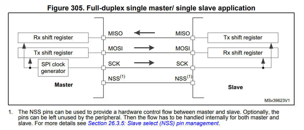
- In Full-duplex mode, all four pins are used
- There are separate pins for send (MOSI) and for receive (MISO)
- When we write data into the Data Register of the master, this data goes into the Tx Shift Register of the master
- Which then gets shifted to the Rx Shift Register of the Slave
- And finally goes into the data register of the slave, from where it is read by the slave device.
Software vs Hardware NSS (Slave Select) in STM32 SPI
STM32 allows two modes to manage NSS (Slave Select):
- Software NSS: You control any GPIO pin manually to select the slave device. This is flexible and often preferred in multi-slave systems.
- Hardware NSS: STM32 handles NSS automatically using the NSS pin. It pulls low when SPI is enabled and high when disabled.
In this tutorial, software NSS is used for better control with ADXL345.
STM32 SPI1 Configuration Using Registers
The configuration for the SPI is relatively simpler than what we have seen in other peripherals. Here we only have to modify 1 register. Let’s see the steps to configure the SPI
/************** STEPS TO FOLLOW *****************
1. Enable SPI clock
2. Configure the Control Register 1
3. Configure the CR2
************************************************/Like I mentioned, it’s very simple to configure the SPI. See the configuration code below
void SPIConfig (void)
{
  RCC->APB2ENR |= (1<<12);  // Enable SPI1 CLock

  SPI1->CR1 |= (1<<0)|(1<<1);   // CPOL=1, CPHA=1

  SPI1->CR1 |= (1<<2);  // Master Mode

  SPI1->CR1 |= (3<<3);  // BR[2:0] = 011: fPCLK/16, PCLK2 = 80MHz, SPI clk = 5MHz

  SPI1->CR1 &= ~(1<<7);  // LSBFIRST = 0, MSB first

  SPI1->CR1 |= (1<<8) | (1<<9);  // SSM=1, SSi=1 -> Software Slave Management

  SPI1->CR1 &= ~(1<<10);  // RXONLY = 0, full-duplex

  SPI1->CR1 &= ~(1<<11);  // DFF=0, 8 bit data

  SPI1->CR2 = 0;
}- First of all enable the SPI 1 clock in the RCC_APB2ENR Register
- Now will modify the CPOL and CPHA bits according to the slave requirement ( watch video if you don’t know what this means)
- Enable the master mode
- Next is the prescalar. The slave device can support upto 5 MBits/s, so I am keeping the presclalar of 16
This will divide the APB2 clock (80 MHz) by 16, and bring it down to 5MHz - The data format is selected as MSB first
- Then we will configure the software slave management. Like I said in the beginning, we will use the software to control the slave, so we need to set these SSM and SSI bits
- Next we will configure the full duplex mode by resetting the RXONLY (10th) bit
- Next is the data length bit, and we will keep the 8 bit data.
- Then reset the entire CR2 register, since we will not be setting up any DMA or Interrupt in this tutorial
STM32 SPI Transmit (Using Data Register)
- Before Transmitting the data, we will wait for the TXE (Transmit Register Empty) bit in the Status Register to set. This indicates that the Transmit Register is empty and we can load the data
- After transmitting the data, we will wait for the BSY (Busy) bit in the Status Register to reset. This will indicate that the SPI is not busy in communication anymore and we can proceed with other things
void SPI_Transmit (uint8_t *data, int size)
{

	/************** STEPS TO FOLLOW *****************
	1. Wait for the TXE bit to set in the Status Register
	2. Write the data to the Data Register
	3. After the data has been transmitted, wait for the BSY bit to reset in Status Register
	4. Clear the Overrun flag by reading DR and SR
	************************************************/

	int i=0;
	while (i<size)
	{
	   while (!((SPI1->SR)&(1<<1))) {};  // wait for TXE bit to set -> This will indicate that the buffer is empty
	   SPI1->DR = data[i];  // load the data into the Data Register
	   i++;
	}


/*During discontinuous communications, there is a 2 APB clock period delay between the
write operation to the SPI_DR register and BSY bit setting. As a consequence it is
mandatory to wait first until TXE is set and then until BSY is cleared after writing the last
data.
*/
	while (!((SPI1->SR)&(1<<1))) {};  // wait for TXE bit to set -> This will indicate that the buffer is empty
	while (((SPI1->SR)&(1<<7))) {};  // wait for BSY bit to Reset -> This will indicate that SPI is not busy in communication

	//  Clear the Overrun flag by reading DR and SR
	uint8_t temp = SPI1->DR;
					temp = SPI1->SR;

}- Here we are waiting for the TXE bit to set before sending the data
- To send the data, we have to copy it in the DR (Data Register)
- After all the data has been transmitted, we will wait for the busy flag to reset
- Before exiting the Transmit function, we will make a dummy read to the data register and the status register.
- This is to clear the overrun flag, which gets set when we transfer the data to the device.
STM32 SPI Receive (Full-Duplex Mode)
The receiving process is as follows:-
- Before receiving the data, we must send some dummy byte to the device. Since the slave device is in the transmission mode, this dummy byte does not change the registers or the data of the registers
- On receiving the dummy byte, the device transmits one byte of data.
- This will set the RXNE (Receive Buffer Not Empty) bit. This will indicate that there is some data in the Data Register, which is ready to be read.
- And later we can copy the data from the Data Register into our buffer. This clears the RXNE bit
void SPI_Receive (uint8_t *data, int size)
{
	/************** STEPS TO FOLLOW *****************
	1. Wait for the BSY bit to reset in Status Register
	2. Send some Dummy data before reading the DATA
	3. Wait for the RXNE bit to Set in the status Register
	4. Read data from Data Register
	************************************************/

	while (size)
	{
		while (((SPI1->SR)&(1<<7))) {};  // wait for BSY bit to Reset -> This will indicate that SPI is not busy in communication
		SPI1->DR = 0;  // send dummy data
		while (!((SPI1->SR) &(1<<0))){};  // Wait for RXNE to set -> This will indicate that the Rx buffer is not empty
	  *data++ = (SPI1->DR);
		size--;
	}
}- As you can see above, we wait for the busy flag to reset.
- Then we send some dummy byte to the device. I am transmitting 0
- next we wait for the RXNE bit to set
- And finally copy the data from the DR into our buffer
STM32 GPIO Configuration for SPI1
STM32F4 GPIO Configuration
I am using the following Pins for the SPI 1:
- PA5 -> CLK
- PA6 -> MISO
- PA7 -> MOSI
- PA9 -> Slave Select
The first three pins need to be set in the alternate function mode, and the PA9 will be set as the general output pin.
The Alternate function mode depends on the microcontroller. For example, let’s see the Alternate function description for F446RE
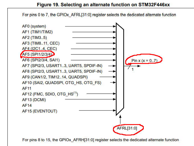
You can see in the picture above that the SPI 1 is the AF5. Also since I am using Pins PA5, 6 and 7, I am going to use the AFRL Register. In case you are using the Pins 8 to 15, you must use the AFRH register
Let’s see the configuration now.
void GPIOConfig (void)
{
	RCC->AHB1ENR |= (1<<0);  // Enable GPIO Clock

	GPIOA->MODER |= (2<<10)|(2<<12)|(2<<14)|(1<<18);  // Alternate functions for PA5, PA6, PA7 and Output for PA9

	GPIOA->OSPEEDR |= (3<<10)|(3<<12)|(3<<14)|(3<<18);  // HIGH Speed for PA5, PA6, PA7, PA9

	GPIOA->AFR[0] |= (5<<20)|(5<<24)|(5<<28);   // AF5(SPI1) for PA5, PA6, PA7
}- First we will enable the GPIOA clock
- Then select the Alternate Function mode for PA5, PA6 and PA7 and the output mode for PA9
- Next we will set the speed for all four pins. The speed is set to HIGH Speed
- And finally configure the Alternate Function in the AFR[0] (AFRL)
STM32F103 GPIO Configuration
The Configuration in F103 is slightly different. F103 do not have the Alternate Function Registers and therefore we have to use the Control Register to configure the SPI pins
Below is the Picture from the F103 Reference manual, suggesting the configuration for the SPI

Since we are using SPI in Master Full Duplex mode, we will configure the pins accordingly. I have already covered how to configure the GPIO in F103, you can check the article STM32F103 Clock Setup using Registers
void GPIOConfig (void)
{
	RCC->APB2ENR |=  (1<<2);  // Enable GPIOA clock
	GPIOA->CRL = 0;
	GPIOA->CRL |= (11U<<20);   // PA5 (SCK) AF output Push Pull
	GPIOA->CRL |= (11U<<28);   // PA7 (MOSI) AF output Push Pull
	GPIOA->CRL |= (1<<26);    // PA6 (MISO) Input mode (floating)
	GPIOA->CRL |= (3<<16);    // PA4 used for CS, GPIO Output
}- Here we will enable the GPIOA clock
- Then reset the entire Control Register
- Now set the AF output Push Pull mode for PA5 -> Clock
- Do the Same for the PA7 -> MOSI
- We need to set the Alternate Function input mode for the PA6 -> MISO
- And set the general Output mode for the PA4 -> SS
How to Interface ADXL345 with STM32 via SPI
Here are some other function that we will be using in this tutorial.
void SPI_Enable (void)
{
	SPI1->CR1 |= (1<<6);   // SPE=1, Peripheral enabled
}

void SPI_Disable (void)
{
	SPI1->CR1 &= ~(1<<6);   // SPE=0, Peripheral Disabled
}

void CS_Enable (void)
{
	GPIOA->BSRR |= (1<<9)<<16;
}

void CS_Disable (void)
{
	GPIOA->BSRR |= (1<<9);
}


float xg, yg, zg;
int16_t x,y,z;
uint8_t RxData[6];

void adxl_write (uint8_t address, uint8_t value)
{
	uint8_t data[2];
	data[0] = address|0x40;  // multibyte write
	data[1] = value;
	CS_Enable ();  // pull the cs pin low
	SPI_Transmit (data, 2);  // write data to register
	CS_Disable ();  // pull the cs pin high
}


void adxl_read (uint8_t address)
{
	address |= 0x80;  // read operation
	address |= 0x40;  // multibyte read
	uint8_t rec;
	CS_Enable ();  // pull the pin low
	SPI_Transmit (&address, 1);  // send address
	SPI_Receive (RxData, 6);  // receive 6 bytes data
	CS_Disable ();;  // pull the pin high
}

void adxl_init (void)
{
	adxl_write (0x31, 0x01);  // data_format range= +- 4g
	adxl_write (0x2d, 0x00);  // reset all bits
	adxl_write (0x2d, 0x08);  // power_cntl measure and wake up 8hz
}Here I am keeping the focus on the SPI, so we will see only the SPI related part. I am not going to talk about how the ADXL actually works. You can check out the other article I wrote about it ADXL345 Accelerometer and STM32
- To ENABLE the SPI, we will set the SPE bit (bit 6 in CR1)
- To DISABLE SPI, we will simply clear that bit
- The slave can be selected by Pulling the SS pin LOW
- And to release the Slave, we have to Pull the SS pin HIGH
In order to communicate with the slave device, we have to follow the procedure as mentioned below
To send the data
- Select the Slave device
- Send the register address
- Send the data
- Release the slave device
To read the data
- Select the slave device
- Send the Register address, from where you want to read
- Read the data
- Unselect the slave device
The main() Function
Below is the main function.
int main ()
{

	SysClockConfig ();
	GPIOConfig ();
	TIM6Config ();
	SPIConfig ();

	SPI_Enable ();

	adxl_init ();

	while (1)
	{
		adxl_read (0x32);
		x = ((RxData[1]<<8)|RxData[0]);
		y = ((RxData[3]<<8)|RxData[2]);
		z = ((RxData[5]<<8)|RxData[4]);

	  xg = x*.0078;
    yg = y*.0078;
   	zg = z*.0078;

		Delay_ms (500);
	}

}- Here we will configure the system, SPI, GPIO etc.
- Then Initialize the ADXL
- Read 6 Bytes of data from the ADXL
- And later convert this data into the acceleration values
In this STM32 SPI tutorial, we implemented full-duplex master communication using only registers. You learned how to transmit and receive bytes using SPI1, configure the NSS pin in software, and communicate with the ADXL345 sensor. Register-based SPI gives you complete control and is perfect for learning low-level peripheral handling.
PROJECT DOWNLOAD
STM32 Register based Tutorial Series

STM32F103 Clock Setup using Registers
STM32 GPIO Output Example Using Registers | BSRR, MODER, GPIOA Explained
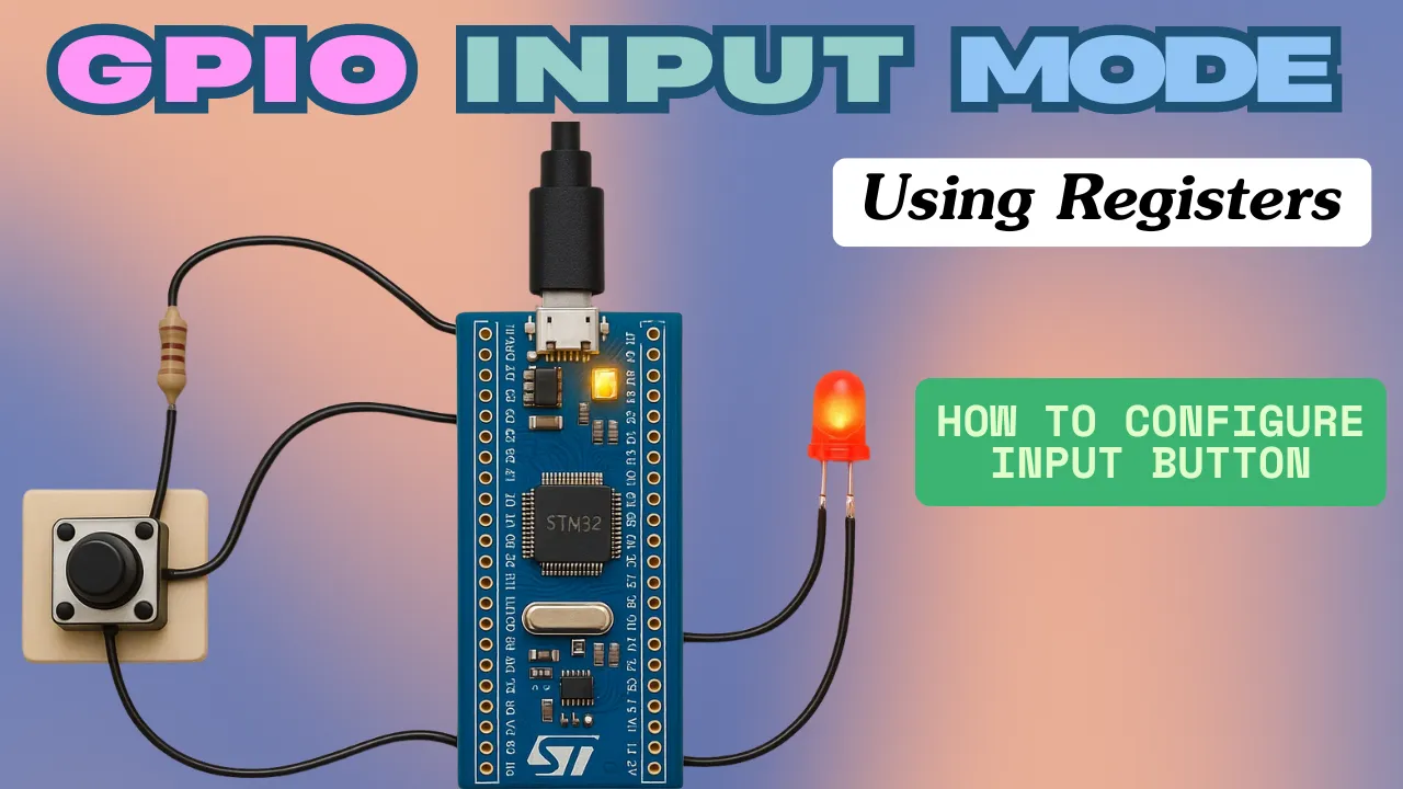
STM32 GPIO Input Configuration – Pin Setup, Pull-Up, and IDR Read
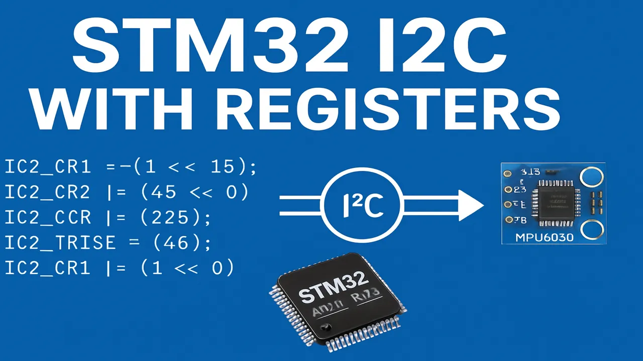
STM32 I2C Tutorial | Register-Based Configuration with Example Code
External Interrupt using Registers

DMA with ADC using Registers in STM32
How to Setup UART using Registers in STM32
Project FAQs


hello , i used the same configuration as you did , the problem is no matter what data i send , i always get another signal in the logic analyser , when i debug the transmission function to see what is written in the data Register , it’s always 0xff, so i thought it might be a problem with the clock thats why i configured the clock with the cube mx not with registers , and i got the same results as before, could you maybe see where the problem might be ? thank you for your efforts .
Hello! Could you please help me with this problem?
ILI9341\ILI9341.axf: Error: L6218E: Undefined symbol __aeabi_assert (referred from touchgfxhal.o).
ILI9341\ILI9341.axf: Error: L6218E: Undefined symbol __aeabi_vec_ctor_nocookie_nodtor (referred from application.o).
ILI9341\ILI9341.axf: Error: L6218E: Undefined symbol typeinfo for touchgfx::Font (referred from constfont.o).
Look like you are missing of touchgfx lib reference on project configure
Thank you so much! Love all of your tutorials. When using an st board as a slave device, I can successfully send data back to the master perfectly at a 1KHz rate. However I cannot check the byte first sent by the master without ruining the synchronization of the spi line. What do I have to do in order to read the byte sent first and then initiate sending the data from the slave? Thanks again