
Home ▸ STM32 Tutorials ▸
Updated On: March 23, 2026
How to Connect and Read ID in W25Q Flash
This tutorial is the start of new series on the W25Q NOR Flash Memories. Throughout this series we will cover different functions to Read, Write, Update and erase the Flash memory. We will cover how to write these function according to the datasheet of the W25Q provided by the winbond.
In today’s tutorial, we will cover how to make the connection with the STM32 controller. Later we will Erase the memory and Read the Device ID.
VIDEO TUTORIAL
You can check the video to see the complete explanation and working of this project.
Connection
The W25Q NOR Flash memories can use the SPI in Single/Dual/Quad mode. For the simplicity of the operation, we will stick to the Single SPI mode, where we would need 4 pins to connect the Flash with the controller.
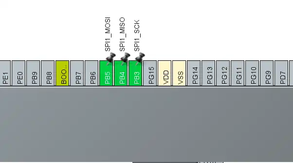
The connection diagram between the Flash module and the STM32 is shown below.
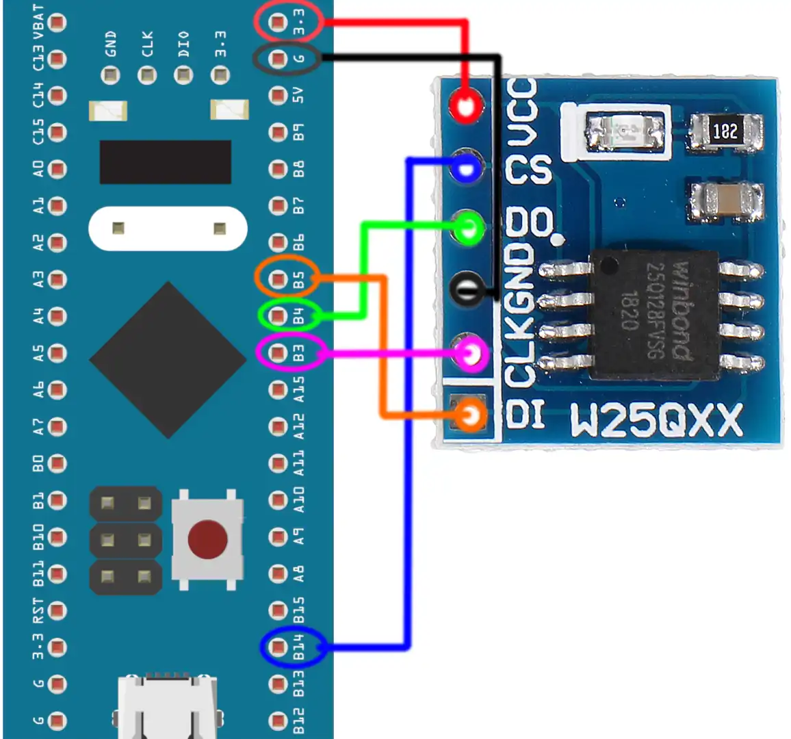
- The CS (Chip Select) Pin is connected to the pin PB14. It will be used to select or unselect the slave Device.
- The DO (Data Out) pin is connected to the pin PB4 (MISO). The device outputs the data on this pin
- The CLK (Clock) pin is connected to the pin PB3 (CLK). The clock is used to synchronise the master and the slave device.
- The DI (Data In) pin is connected to the pin PB5 (MOSI). The master send the data to the device on this pin.
- The Device is powered with 3.3v from the MCU itself.
The Module provides 6 pins (including the Vcc and Gnd). But the chip has 8 pins in total. If you have the chip rather than the module, you can connect it as shown below.
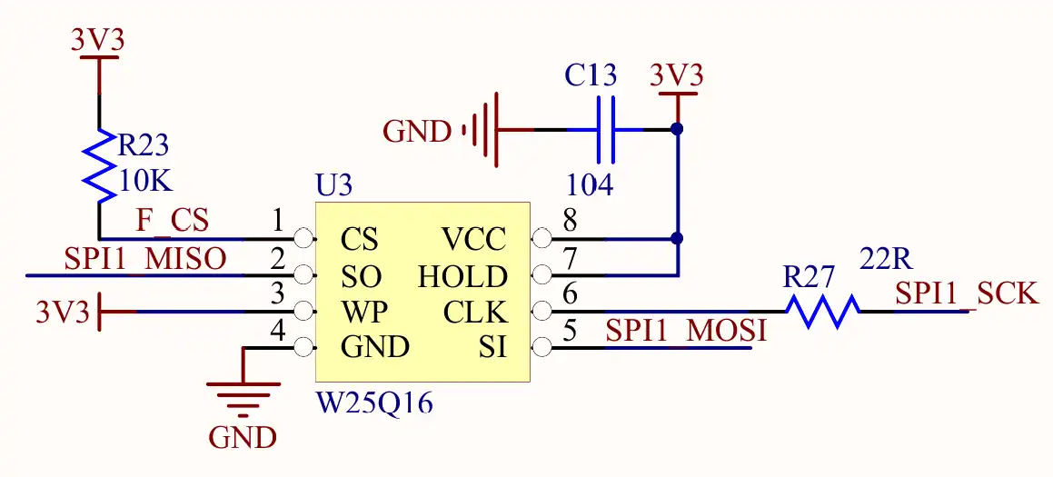
Note that the WP (Write Protect) pin is active Low pin, so it must be pulled HIGH when you want to modify the flash, and pulled LOW when you want to disable the modification.
The connections shown above are for the Single SPI mode, not for Dual or Quad modes.
CubeMX Setup
We will enable the SPI in Full Duplex master mode. The configuration is shown below.
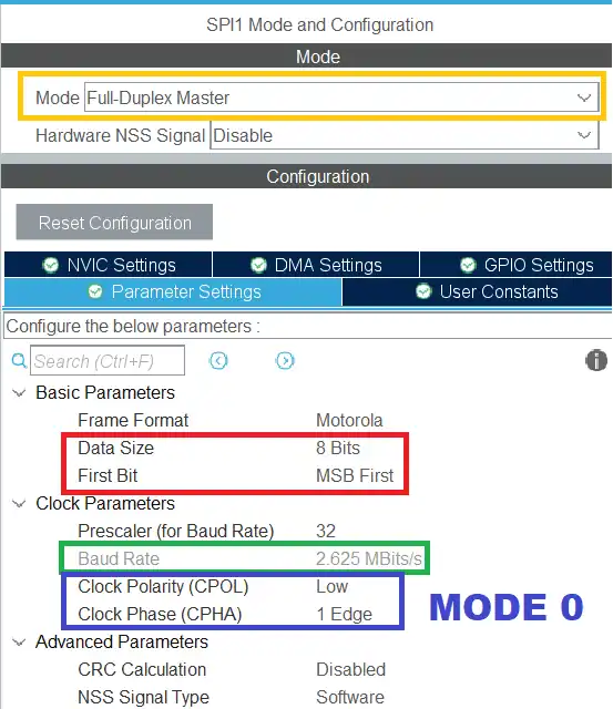
The Data width is set to 8 bits and the data should be transferred as the MSB first. The prescaler is set such that the Baud Rate is around 2.5 Mbits/sec.
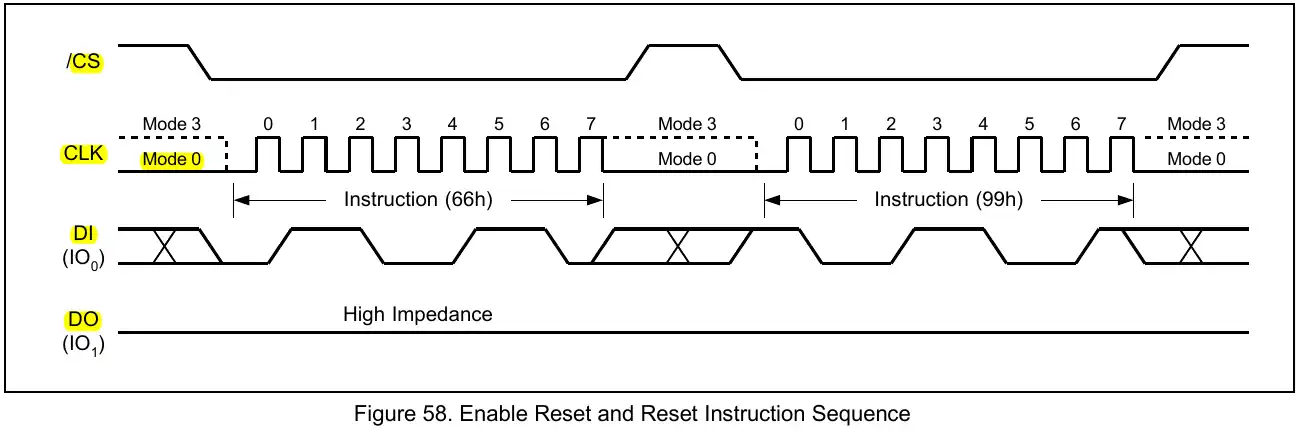
According to the datasheet of the W25Q Flash, the SPI Mode 0 and Mode 3 are supported. Below is the image from the datasheet.
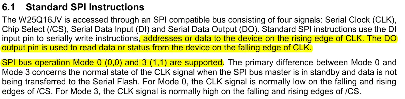
In the SPI configuration, we keep the Clock Polarity (CPOL) low and the Clock Phase (CPHA) to 1 edge. Here 1 edge means that the data will be sampled on the first edge of the clock. And when the CPOL is Low, the first edge is the rising edge. Basically we are using the SPI Mode 0.
In Full duplex Mode, SPI uses 3 pins, MOSI, MISO and CLK. We need to set one more pin as output so to be used as the Chip Select (CS) Pin.
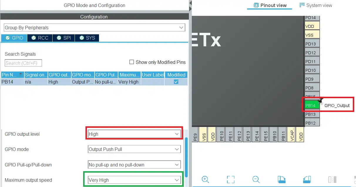
The Pin PB14 is set as the CS pin. The initial output level is set to HIGH. This is because the pin needs to be pulled low in order to select the slave device, so we keep it high initially to make sure the slave device isn’t selected. The Output speed is set to Very High because we might need to select and unselect the slave at higher rate.
Let’s Write the Code
We will create separate library files for the device. And later in the upcoming tutorials, we will simply update the code in these files itself.
I have created the W25Qxx.c file in the src directory and W25Qxx.h file in the Inc directory.
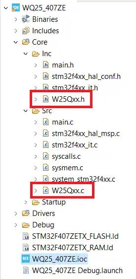
We will write our functions in the W25Qxx.c file.
Some Definitions
#include "main.h"
#include "W25Qxx.h"

extern SPI_HandleTypeDef hspi1;
#define W25Q_SPI hspi1
#define W25Q_Delay (uint32_t time) HAL_Delay (time)First include the main header file and the W25Qxx header file. The SPI handler is defined in the main.c file, so we copy it here as an external variable. I have defined the SPI1 handler as the W25Q_SPI.
I am also defining a delay function in case we need to use the delay in the code. The implementation of the delay function can be changed based on what MCU you are using.
The chip select pin needs to be pulled High and Low whenever we want to read or write the data to the device. So we define the chip select functions separately.
void csLOW(void)
{
	HAL_GPIO_WritePin(GPIOB, GPIO_PIN_14, GPIO_PIN_RESET);
}

void csHIGH(void)
{
	HAL_GPIO_WritePin(GPIOB, GPIO_PIN_14, GPIO_PIN_SET);
}The pin PB14 is connected to the CS pin of the device. The csLOW() function will simply pull the pin PB14 Low and csHIGH() will pull it High.
We will also define the SPI Read and Write functions. This will make it easier to modify the code for different MCUs without having to modify a lot in the code.
void SPI_Write (uint8_t *data, uint8_t len)
{
	HAL_SPI_Transmit(&W25Q_SPI, data, len, 2000);
}

void SPI_Read (uint8_t *data, uint8_t len)
{
	HAL_SPI_Receive(&W25Q_SPI, data, len, 5000);
}The parameter for the SPI_Write function is pointer to the data to be transmitted and the length of the data. It then passes the same parameters to the HAL_SPI_Transmit function.
Similarly, the SPI_Read function reads the “len” number of bytes, and store them in the array whose address is passed to the function.
Resetting the Chip
Before starting a ne session with the chip we should reset it. This would terminate any on going operation and the device will return to its default power-on state. It will lose all the current volatile settings, such as Volatile Status Register bits, Write Enable Latch (WEL) status, Program/Erase Suspend status, Read parameter setting (P7-P0) and Wrap Bit setting (W6-W4).
To avoid the accidental Reset, a Reset command is made of 2 instructions. these Instructions, “Enable Reset (66h)” and “Reset (99h)” must be issues in a sequence. Once the Reset command is accepted by the device, the device will take approximately 30us to reset. During this period, no command will be accepted.
We will write a separate function to reset the chip. The code is shown below
void W25Q_Reset (void)
{
	uint8_t tData[2];

	tData[0] = 0x66;  // enable Reset
	tData[1] = 0x99;  // Reset
        csLOW();
	SPI_Write(tData, 2);
	csHIGH(); // pull the HIGH
        W25Q_Delay (100);
}- Since we need to send 2 instructions, we define an array of 2 bytes.
- Then store the instructions in sequence with Enable Reset followed by the Reset Instruction.
- Pull the CS Low to select the device, send the 2 bytes data using SPI_Write and Pull the CS High to unselect the device.
- Provide 100ms delay so that the things can settle after the reset.
Reading ID
We will also Read the ID of the device in today’s tutorial. The W25Q series devices are equipped with different IDs like manufacturer ID, Device ID, Unique ID and JEDEC ID. We will read the JEDEC ID as it give a lot of useful information about the device.
The instruction 9Fh can be used to read the JEDEC ID.
The JEDEC assigned Manufacturer ID byte for Winbond (EFh) and two Device ID bytes, Memory Type (ID15-ID8) and Capacity (ID7-ID0) are then shifted out on the falling edge of CLK with most significant bit (MSB) first.
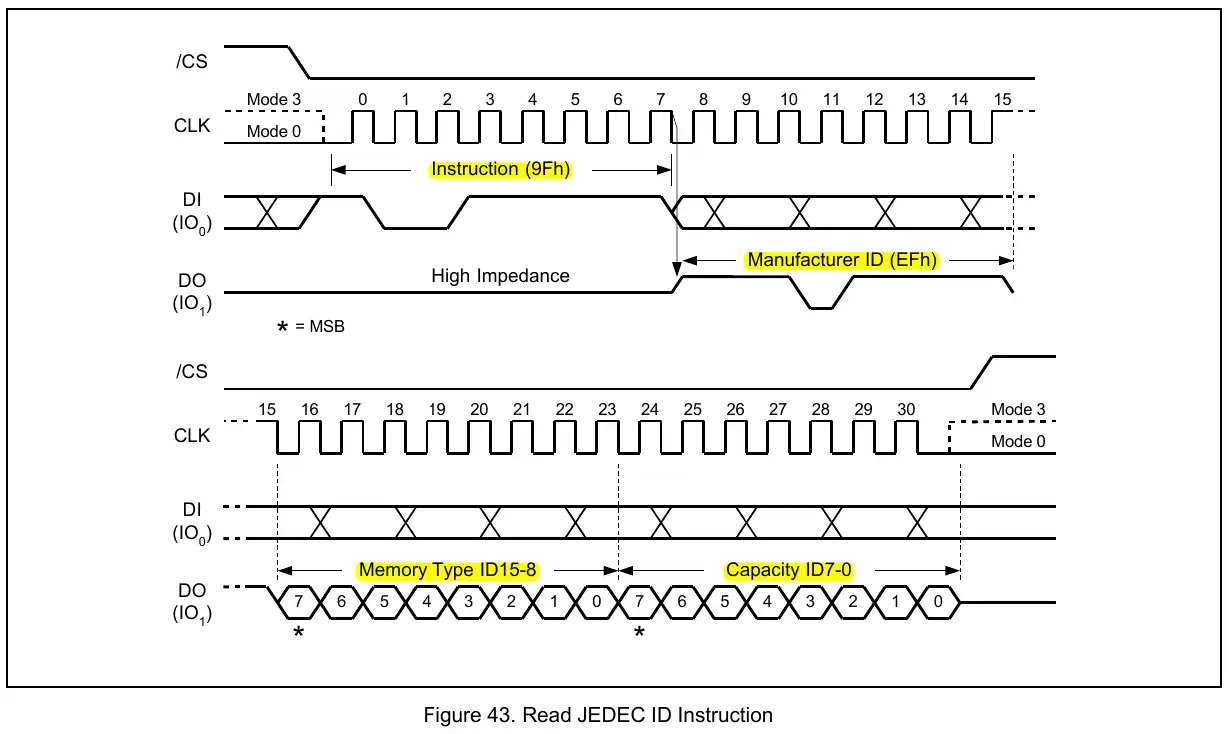
The manufacturer ID (EFh) remains same across all the winbond flash memories. The Memory Type ID and the Capacity ID changes based on what device you are using.
I have the W25Q16JV chip, which is 16 Megabits in size. The ID for this chip is shown below.
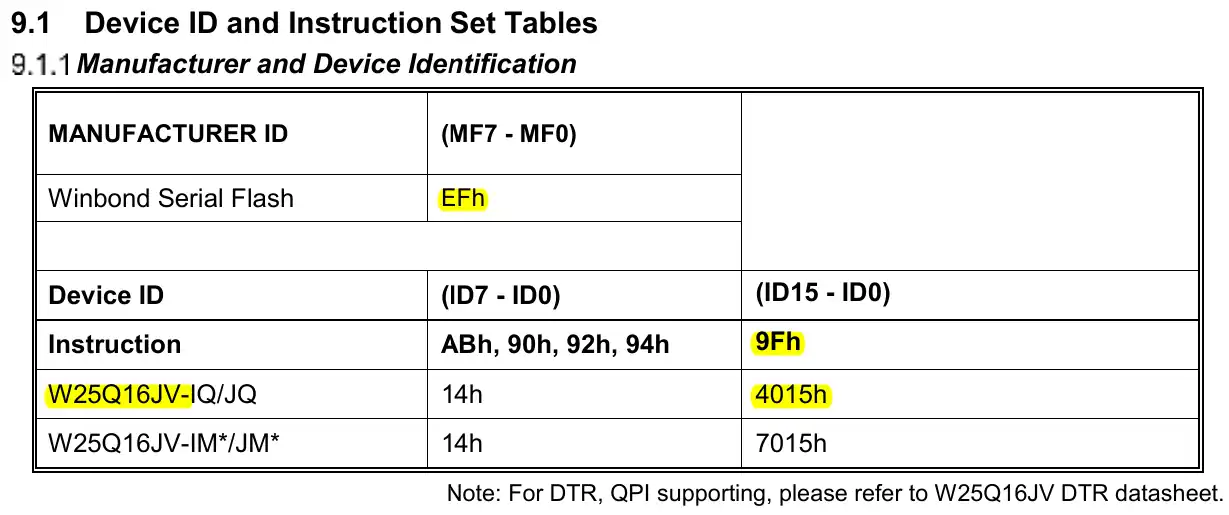
The Manufacturer ID is 0xEF and the 2 device ID bytes are going to be 0x4015. Below is the function to read the ID.
uint32_t W25Q_ReadID (void)
{
	uint8_t tData = 0x9f;  // Read ID
	uint8_t rData[3];
	csLOW();  // pull the CS LOW
	SPI_Write(&tData, 1);
	SPI_Read(rData, 3);
	csHIGH();  // pull the HIGH
	return ((rData[0]<<16)|(rData[1]<<8)|rData[2]); // MFN ID : MEM ID : CAPACITY ID
}We define a variable and store the instruction (0x9F) to Read the ID. The array rData is used to store the 3 received bytes.
Then send the instruction using SPI_Write() function and read 3 bytes using the SPI_Read() function.
The rData[0] stores the Manufacturer ID, rData[1] stores the Memory ID and the rData[2] stores the Capacity ID. We combine the 3 bytes and make a final 24 bit ID in the format MFN ID : MEM ID : CAPACITY ID. Finally return the 24 bit ID.
The main function
In the main function define a 32 bit variable to store the ID. The we reset the Device and Read the ID.
uint32_t ID = 0;
int main ()
{
  ......
  W25Q_Reset();
  ID = W25Q_ReadID();
  ......
}Result
Below is the image showing the ID in the Live Expression.
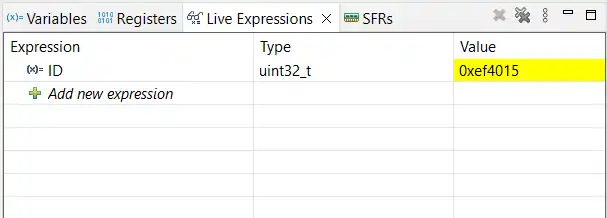
The 24 bit ID is 0xEF4015. This is as per the information provided in the datasheet.
STM32 W25Q Flash Tutorials Series
W25Q Flash Series Part 3 – How to Erase Sectors

W25Q Flash Series Part 4 – How to Program Pages
W25Q Flash Series Part 5 – how to update sectors

W25Q Flash Series Part 6 – Integers floats and 32bit Data

W25Q Flash Series Part 7 – QUADSPI Write, Read, Memory Mapped mode
W25Q Flash Series Part 8 – QUADSPI External Loader
W25Q Flash Series Part 9 – SPI Flash Loader


can i use this tutorial for (stm32u5g7vjt6 with MT25QL128A) external NOR Flash assets by Touch GFX
No you can not. This is exclusive to W25Q Flash memory.
You can take a look at the other QSPI video for N25Q Flash memeory https://youtu.be/gAyuF20ok8c
You are amazing
If anyone is struggling to get this working try
https://stm32world.com/wiki/STM32_W25Qxx
Github Library:- https://github.com/mengguang/w25qxx/tree/master
As the ReadID worked 100% with this library.
hello Mr.controllersTech
I’m trying to read the ID of my flash W25Q16jv, it returns the TYPE but no VALUE
I have stm32f103RCT6 mini v2.0
Use short wires for connection