Home ▸ STM32 Tutorials ▸
Updated On: March 23, 2026
STM32 I2C Tutorial | Register-Based Configuration with Example Code
Welcome to this STM32 I2C tutorial. In this guide, we’ll configure I2C using register-level programming on STM32 microcontrollers. This STM32 I2C example focuses on both transmission and reception using direct register access (not HAL). Whether you’re searching for STM32 I2C example code, register details, or step-by-step configuration—this tutorial has you covered.
This is another tutorial in Register based series for STM32, and it will explain how to configure I2C on STM32 using only registers. It will cover clock and GPIO setup, timing configuration, and basic I2C functions like start, read, write, and stop. It will also include an example of interfacing the MPU6050 sensor to read accelerometer data.
I will cover both transmission and reception using the I2C. The configuration will remain common in both the processes.
VIDEO TUTORIAL
You can check the video to see the complete explanation and working of this project.
STM32 I2C Configuration
The steps below are required to configure the I2C in STM32F4 Microcontroller.
/**** STEPS FOLLOWED  ************
1. Enable the I2C CLOCK and GPIO CLOCK
2. Configure the I2C PINs for ALternate Functions
	a) Select Alternate Function in MODER Register
	b) Select Open Drain Output
	c) Select High SPEED for the PINs
	d) Select Pull-up for both the Pins
	e) Configure the Alternate Function in AFR Register
3. Reset the I2C
4. Program the peripheral input clock in I2C_CR2 Register in order to generate correct timings
5. Configure the clock control registers
6. Configure the rise time register
7. Program the I2C_CR1 register to enable the peripheral
*/Let’s cover them one by one.
1. Enable the I2C and GPIO CLOCKS
I2C CLOCK can be enabled in the RCC_APB1ENR Register
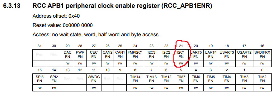
As you can see above, the I2C1 Enable Bit is 21st bit of the RCC_APB1ENR Register. And in order to enable the clock, we need to write a ‘1’ in this position
RCC->APB1ENR |= (1<<21); // enable I2C CLOCKSimilarly we will enable the GPIO clock also. I2C1 is connected to pins PB8 and PB9 and therefore we will enable the GPIOB clock in RCC_AHB1ENR Register
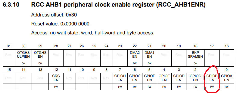
GPIOB Enable Bit is 1st bit of RCC_AHB1ENR Register
RCC->AHB1ENR |= (1<<1); // Enable GPIOB CLOCK2. Configure the Pins for I2C
Configuring the pins is divided to various steps:
Select Alternate Function in MODER Register
The MODER Register can be used to configure the pins in different modes.
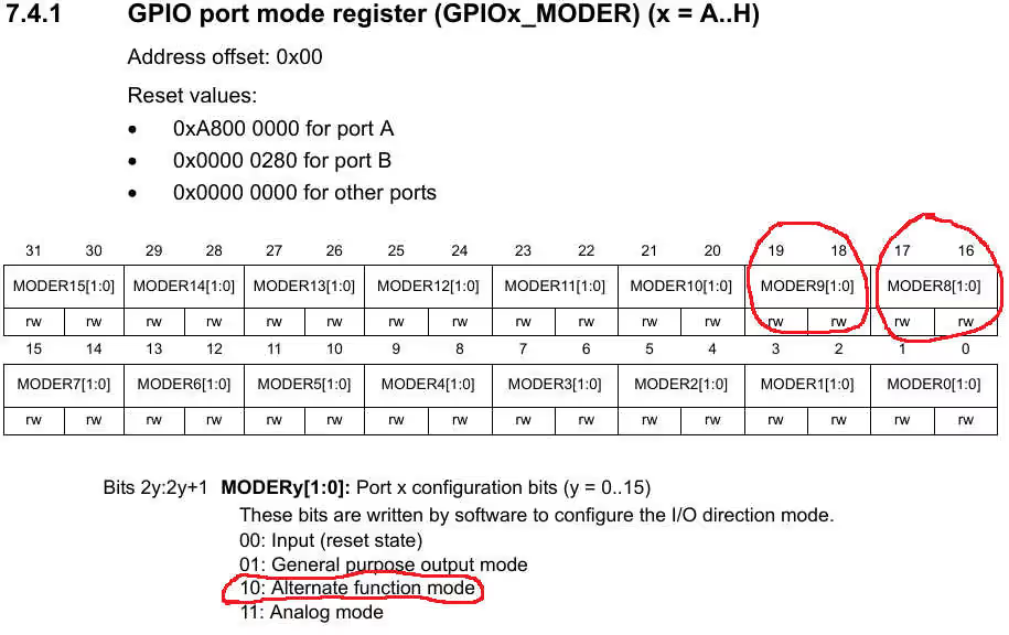
As I am using Pins PB8 and PB9 for the I2C (Alternate functions), I need to set the Bits (17:16) = 1:0 for PB8 and Bits (19:18) = 1:0 for PB9.
GPIOB->MODER |= (2<<16) | (2<<18); // Bits (17:16)= 1:0 --> Alternate Function for Pin PB8; Bits (19:18)= 1:0 --> Alternate Function for Pin PB9Select Open Drain Output
The OTYPER Register can be used to select the output type.
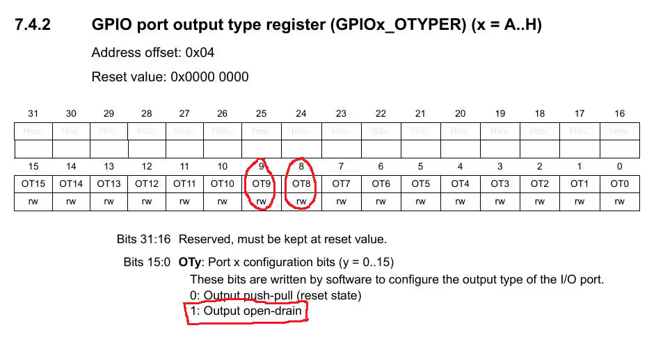
To select the Pin as the output drain we need to write a ‘1’ in the 8th and 9th bits (PB8, PB9).
GPIOB->OTYPER |= (1<<8) | (1<<9); // Bit8=1, Bit9=1 output open drainSelect High SPEED for the PINs
The speed selection can be done using OSPEEDR Register
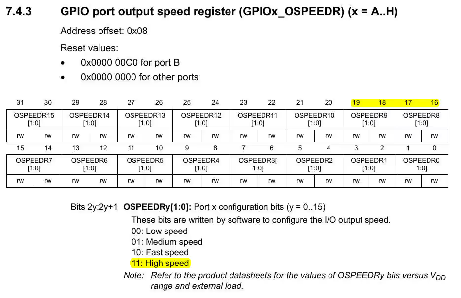
We will select the High Speed for both of our pins here Bits (17:16)= 1:1 (for PB8) and Bits (19:18)= 1:1 for PB9.
GPIOB->OSPEEDR |= (3<<16) | (3<<18); // Bits (17:16)= 1:1 --> High Speed for PIN PB8; Bits (19:18)= 1:1 --> High Speed for PIN PB9Select Pull-up for both the Pins
It’s better to use external pull up registers while using I2C, but just for the sake of this tutorial I am using internal pull-up resistors.
The Internal Pull up registers can be controlled by using PUDPR Register.
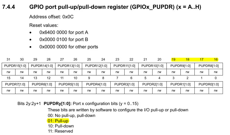
Inorder to enable the Pull-Up resistors, we need to write Bits (17:16)= 0:1 for PB8, and Bits (19:18)= 0:1 for PB9.
GPIOB->PUPDR |= (1<<16) | (1<<18); // Bits (17:16)= 0:1 --> Pull up for PIN PB8; Bits (19:18)= 0:1 --> pull up for PIN PB9Configure the Alternate Function in AFR Register
We have already set the pins in the alternate functions mode, but we haven’t defined what those functions should be. This can be done by modifying the AFR Registers.
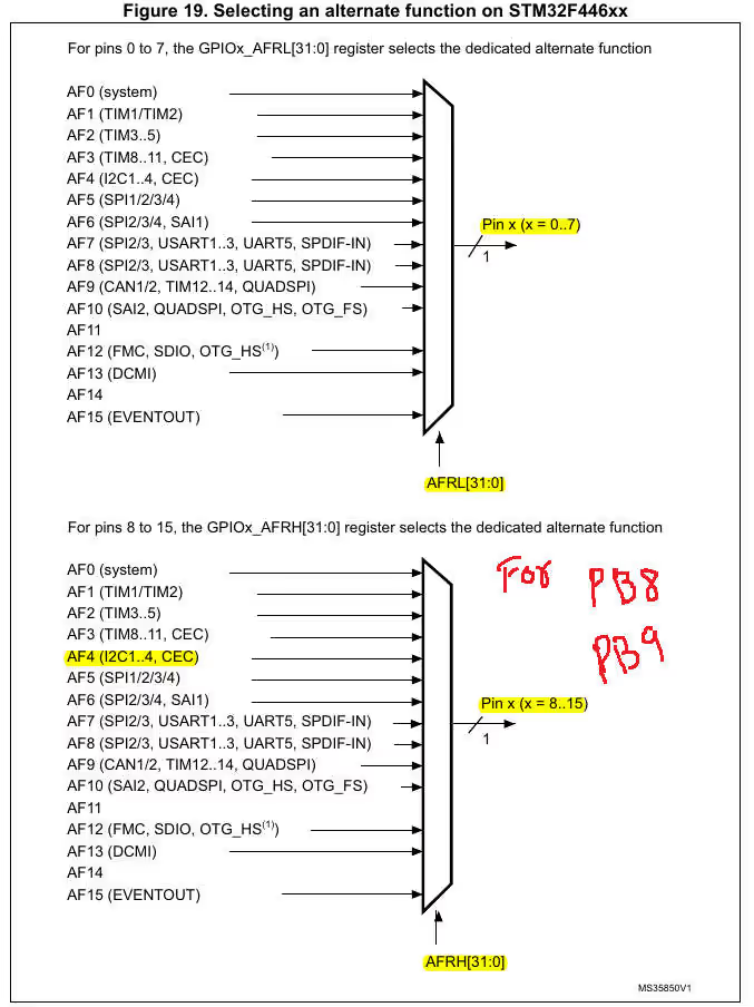
AFR Register is divided into 2 sections i.e AFRH (Pins 8 to 15) and AFRL (Pins 0 to 7).
Since I am using Pins PB8 and PB9, I will be modifying AFRH.
As you can see above, AF4 is the function corresponding to the I2C1. Also AFRH is shown below.
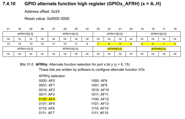
Inorder to set the function AF4, we need to write Bits (3:2:1:0) = 0:1:0:0 for PB8, and Bits (7:6:5:4) = 0:1:0:0 for PB9
GPIOB->AFR[1] |= (4<<0) | (4<<4); // Bits (3:2:1:0) = 0:1:0:0 --> AF4 for pin PB8; Bits (7:6:5:4) = 0:1:0:0 --> AF4 for pin PB9This completes the Configuration of the Pins for the I2C. Now we will configure the rest of the I2C using I2C Registers
3. Reset the I2C
In order to reset the I2C, we need to modify the I2C Control Register 1 (I2C_CR1).
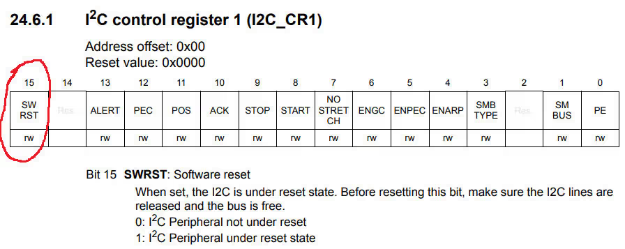
As you can see above the 15th bit of this register is the SWRST (Software reset). We will write a ‘1’ to this position to reset the I2C, and again write a ‘0’ to this position to pull the I2C from the reset
I2C1->CR1 |= (1<<15);  // reset the I2C
I2C1->CR1 &= ~(1<<15); // Normal operation4. Set the I2C clock
Now we need to set the 1000 KHz clock for the I2C and the formula for the same in the reference manual is shown below.
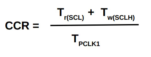
Here the values of Tr(scl) and Tw(sclh) are provided in the datasheet as you can see below
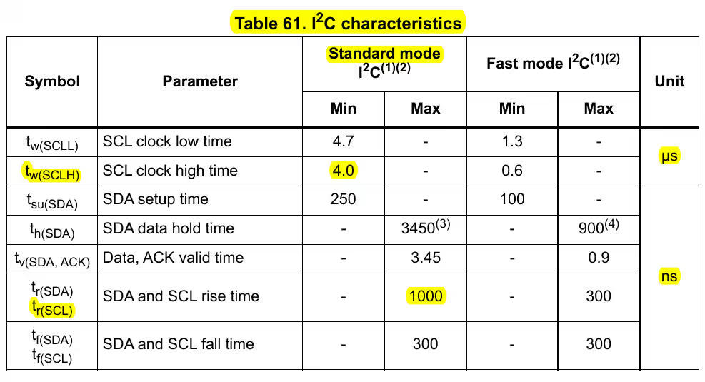
TPCLK1 is the Time Period for the Peripheral clock. We need to set the value of the peripheral clock in the I2C Control Register 2 (I2C_CR2). The Clock setup from the first tutorial is shown below
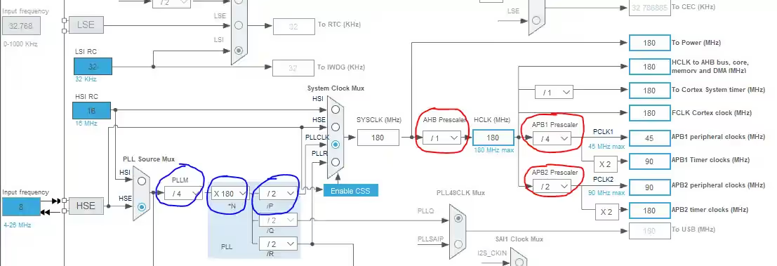
As you can see the APB1 Peripheral Clock is at 45 MHz, and that’s the value we are going to input in the I2C_CR2 Register
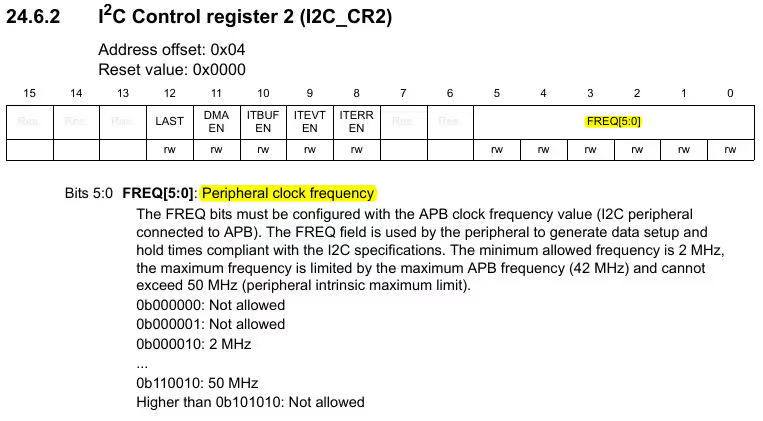
// Program the peripheral input clock in I2C_CR2 Register in order to generate correct timings
I2C1->CR2 |= (45<<0); // PCLK1 FREQUENCY in MHzUsing all the above values in the mentioned formula, gives us the value for the Clock Control Register (CCR)
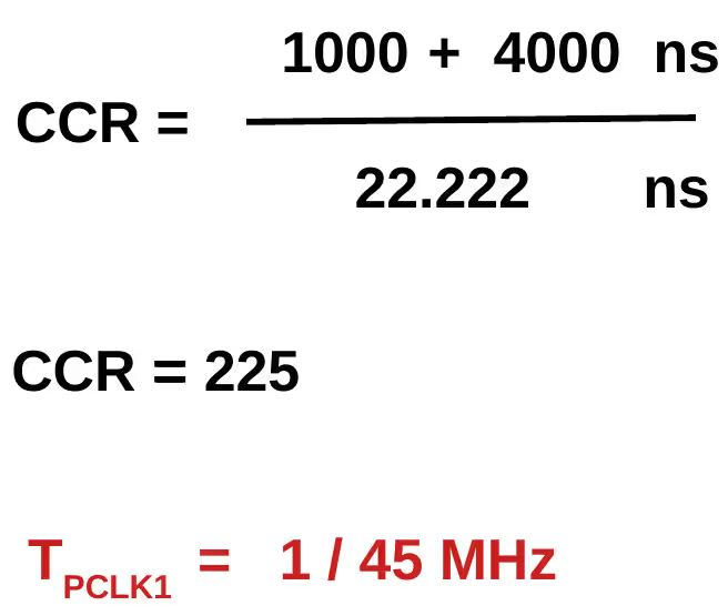
Now we feed this value to the CCR Register
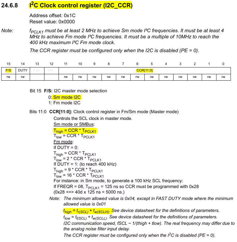
// Configure the clock control registers
I2C1->CCR = 225<<0; // check calculation in PDFAfter CCR, we will program the TRISE Register (I2C_TRISE). The formula to calculate TRISE value is shown below
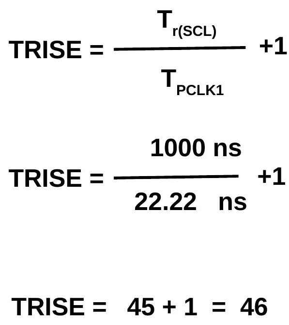
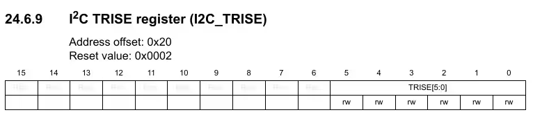
// Configure the rise time register
I2C1->TRISE = 46; // check PDF againThis completes the Setup for the I2C Clock. Now we will enable the I2C
4. Enable the I2C
The I2C Peripheral can be enabled in the Control Register 1 (I2C_CR1). The Register is shown below
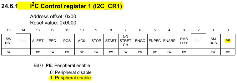
PE is the Peripheral Enable bit, and to enable or disable the I2C, we need to modify this bit.
// Program the I2C_CR1 register to enable the peripheral
I2C1->CR1 |= (1<<0); // Enable I2CThis completes the configuration for the I2C. Now we will cover all the I2C functions that we are going to use, in order to write or read the data from any I2C device
STM32 I2C Example Code Using Registers
The following I2C example for STM32 covers how to manually implement I2C communication using low-level registers. No HAL or CubeMX is used. These examples are tested on STM32F4 series and work with peripherals like MPU6050.
We are going to create different functions to interact with the I2C device. Let’s see them
I2C START
I2C_Start will be used to start the I2C Communication. Following are the steps required to start the I2C
/**** STEPS FOLLOWED  ************
1. Enable the ACK
2. Send the START condition
3. Wait for the SB ( Bit 0 in SR1) to set. This indicates that the start condition is generated
*/ First of all we will enable the ACK bit and send the start condition. These both can be done by modifying the Control Register 1 (I2C_CR1)
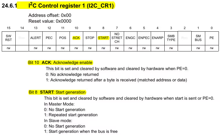
I2C1->CR1 |= (1<<10);  // Enable the ACK
I2C1->CR1 |= (1<<8); // Generate STARTThis will generate the START condition on the I2C bus
I2C WRITE
I2C_Write can be used to write the data to the slave device. The following is the procedure to perform the I2C Write
/**** STEPS FOLLOWED  ************
1. Wait for the TXE (bit 7 in SR1) to set. This indicates that the DR is empty
2. Send the DATA to the DR Register
3. Wait for the BTF (bit 2 in SR1) to set. This indicates the end of LAST DATA transmission
*/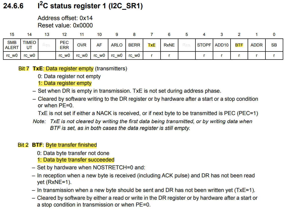
while (!(I2C1->SR1 & (1<<7)));  // wait for TXE bit to set
I2C1->DR = data;
while (!(I2C1->SR1 & (1<<2))); // wait for BTF bit to set- Here we first wait for the TXE (bit 7 in SR1) to set. This bit indicates that the DR (Data Register) is Empty.
- Then we copy the Data into the DR.
- And finally we wait for the BTF (Bit 2 in SR1) to set. This will indicate that the Byte transfer has finished.
This completes the write process.
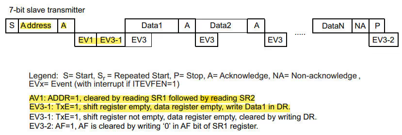
Send Slave Address
Generally Sending Address can be handled by the write function, but ST have slightly different checks for the Address alone. This is why I have created a separate function to deal with the Address part.
/**** STEPS FOLLOWED  ************
1. Send the Slave Address to the DR Register
2. Wait for the ADDR (bit 1 in SR1) to set. This indicates the end of address transmission
3. clear the ADDR by reading the SR1 and SR2
*/ 
I2C1->DR = Address;  //  send the address
while (!(I2C1->SR1 & (1<<1)));  // wait for ADDR bit to set
uint8_t temp = I2C1->SR1 | I2C1->SR2; // read SR1 and SR2 to clear the ADDR bit- Here we first send the Address of the slave Device by copying it into the DR (Data Register).
- Then we wait for the ADDR (Bit 1 in SR1) to set. This will indicate that the Address Transmission is finished.
- Now we will clear the ADDR bit by performing a dummy read in Status Registers SR1 and SR2.
This will complete the Address Transmission. You can Read the ACK flag after this step to confirm whether the slave device has sent the acknowledgement or not.
I2C READ
I2C_Read is probably the most complicated part. It is used to read the data from the device. Let’s see the detail about the steps
/**** STEPS FOLLOWED  ************
1. If only 1 BYTE needs to be Read
	a) Write the slave Address, and wait for the ADDR bit (bit 1 in SR1) to be set
	b) the Acknowledge disable is made during EV6 (before ADDR flag is cleared) and the STOP condition generation is made after EV6
	c) Wait for the RXNE (Receive Buffer not Empty) bit to set
	d) Read the data from the DR

2. If Multiple BYTES needs to be read
  a) Write the slave Address, and wait for the ADDR bit (bit 1 in SR1) to be set
	b) Clear the ADDR bit by reading the SR1 and SR2 Registers
	c) Wait for the RXNE (Receive buffer not empty) bit to set
	d) Read the data from the DR
	e) Generate the Acknowlegment by settint the ACK (bit 10 in SR1)
	f) To generate the nonacknowledge pulse after the last received data byte, the ACK bit must be cleared just after reading the
		 second last data byte (after second last RxNE event)
	g) In order to generate the Stop/Restart condition, software must set the STOP/START bit
	   after reading the second last data byte (after the second last RxNE event)
*/int remaining = size;
/**** STEP 1 ****/
if (size == 1)
{
/**** STEP 1-a ****/
I2C1->DR = Address; // send the address
while (!(I2C1->SR1 & (1<<1))); // wait for ADDR bit to set
/**** STEP 1-b ****/
I2C1->CR1 &= ~(1<<10);  // clear the ACK bit
uint8_t temp = I2C1->SR1 | I2C1->SR2;  // read SR1 and SR2 to clear the ADDR bit.... EV6 condition
I2C1->CR1 |= (1<<9);  // Stop I2C
/**** STEP 1-c ****/
while (!(I2C1->SR1 & (1<<6))); // wait for RxNE to set
/**** STEP 1-d ****/
buffer[size-remaining] = I2C1->DR; // Read the data from the DATA REGISTER
}
/**** STEP 2 ****/
else
{
/**** STEP 2-a ****/
I2C1->DR = Address; // send the address
while (!(I2C1->SR1 & (1<<1))); // wait for ADDR bit to set
/**** STEP 2-b ****/
uint8_t temp = I2C1->SR1 | I2C1->SR2; // read SR1 and SR2 to clear the ADDR bit
while (remaining>2)
{
/**** STEP 2-c ****/
while (!(I2C1->SR1 & (1<<6))); // wait for RxNE to set
/**** STEP 2-d ****/
buffer[size-remaining] = I2C1->DR; // copy the data into the buffer
/**** STEP 2-e ****/
I2C1->CR1 |= 1<<10; // Set the ACK bit to Acknowledge the data received
remaining--;
}
// Read the SECOND LAST BYTE
while (!(I2C1->SR1 & (1<<6))); // wait for RxNE to set
buffer[size-remaining] = I2C1->DR;
/**** STEP 2-f ****/
I2C1->CR1 &= ~(1<<10); // clear the ACK bit
/**** STEP 2-g ****/
I2C1->CR1 |= (1<<9); // Stop I2C
remaining--;
// Read the Last BYTE
while (!(I2C1->SR1 & (1<<6))); // wait for RxNE to set
buffer[size-remaining] = I2C1->DR; // copy the data into the buffer
} Before we discuss this in more details, there are few common things in reading the data here
- After sending the read address, we always wait for the ADDR (Bit 1 in SR1) to set. This indicates that the address has been transmitted
- Before Reading the data from the DR (Data Register), we always wait for the RXNE (Bit 6 in SR1) to set. This indicates that the Receive buffer is not empty, and it is ready to be read.
This Read function is divided into 2 different parts. If you want to read a single byte, or multiple bytes. The reason for this is as shown below
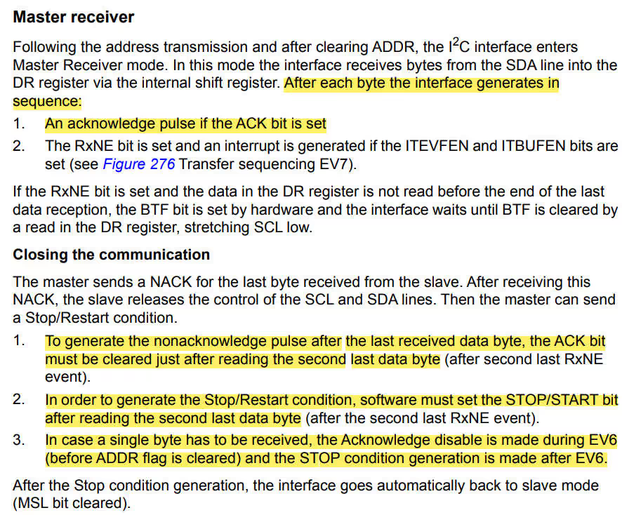
If we are going to receive only a single byte, we need to send the ACK Disable before clearing the Address flag, and the STOP condition after disabling the flag. This can be seen in the code below
/**** STEP 1-b ****/
I2C1->CR1 &= ~(1<<10);  // clear the ACK bit
uint8_t temp = I2C1->SR1 | I2C1->SR2;  // read SR1 and SR2 to clear the ADDR bit.... EV6 condition
I2C1->CR1 |= (1<<9);  // Stop I2C
Things are different for multiple byte reception. Here we need to send the ACK Disable and STOP conditions after receiving the second last data byte. This can be seen below
while (remaining>2)
{
	/**** STEP 2-c ****/
	while (!(I2C1->SR1 & (1<<6)));  // wait for RxNE to set

	/**** STEP 2-d ****/
	buffer[size-remaining] = I2C1->DR;  // copy the data into the buffer

	/**** STEP 2-e ****/
	I2C1->CR1 |= 1<<10;  // Set the ACK bit to Acknowledge the data received

	remaining--;
}

// Read the SECOND LAST BYTE
while (!(I2C1->SR1 & (1<<6)));  // wait for RxNE to set
buffer[size-remaining] = I2C1->DR;

/**** STEP 2-f ****/
I2C1->CR1 &= ~(1<<10);  // clear the ACK bit

/**** STEP 2-g ****/
I2C1->CR1 |= (1<<9);  // Stop I2C

remaining--;

// Read the Last BYTE
while (!(I2C1->SR1 & (1<<6)));  // wait for RxNE to set
buffer[size-remaining] = I2C1->DR; // copy the data into the buffer- Till the remaining bytes are more than 2, we will perform the simple reception. Where we read the data from the DR and send an ACK after reading this data
- But when we receive the second last data byte, we will send the ACK Disable and STOP, to indicate that we want to end the reception after the next data byte
- Now we will read the last data byte and the I2C will automatically stop after that
This completes the I2C related functions, Now let’s see the Process of writing and Receiving data
How to use the I2C Functions
Here we will discuss how can we use the functions that we have created above. I am going to create 2 separate functions for writing and reading the data from the slave device. I am going to use MPU6050 for demonstration.
Write Data to Slave Device
The process of writing the data to any I2C Device is mentioned below.
/**** STEPS FOLLOWED  ************
1. START the I2C
2. Send the ADDRESS of the Device
3. Send the ADDRESS of the Register, where you want to write the data to
4. Send the DATA
5. STOP the I2C
*/The function below will write the data to the slave device.
void MPU_Write (uint8_t Address, uint8_t Reg, uint8_t Data)
{
	I2C_Start ();
	I2C_Address (Address);
	I2C_Write (Reg);
	I2C_Write (Data);
	I2C_Stop ();
}Read Data from Slave Device
The reading process is also similar, but with a few more extra steps. It is shown below.
/**** STEPS FOLLOWED  ************
1. START the I2C
2. Send the ADDRESS of the Device
3. Send the ADDRESS of the Register, where you want to READ the data from
4. Send the RESTART condition
5. Send the Address (READ) of the device
6. Read the data
7. STOP the I2C
*/The function below will read the data from the slave device.
void MPU_Read (uint8_t Address, uint8_t Reg, uint8_t *buffer, uint8_t size)
{
	I2C_Start ();
	I2C_Address (Address);
	I2C_Write (Reg);
	I2C_Start ();  // repeated start
	I2C_Read (Address+0x01, buffer, size);
	I2C_Stop ();
}Here MPU_Read is the function to read the data from the device. Note that the Slave Address is (Address+0x01) during the Read function. Basically we need to set the R/W bit (Bit 0) HIGH during the Read operation. This is common for all the devices that you will use for the I2C.
The main Function
I have already covered how to Read the data from MPU6050. We are not going to cover it in detail here. The main function below just demonstrates that the I2C functions actually works.
void MPU6050_Init (void)
{
uint8_t check;
uint8_t Data;
// check device ID WHO_AM_I
MPU_Read (MPU6050_ADDR,WHO_AM_I_REG, &check, 1);
if (check == 104) // 0x68 will be returned by the sensor if everything goes well
{
// power management register 0X6B we should write all 0's to wake the sensor up
Data = 0;
MPU_Write (MPU6050_ADDR, PWR_MGMT_1_REG, Data);
// Set DATA RATE of 1KHz by writing SMPLRT_DIV register
Data = 0x07;
MPU_Write(MPU6050_ADDR, SMPLRT_DIV_REG, Data);
// Set accelerometer configuration in ACCEL_CONFIG Register
// XA_ST=0,YA_ST=0,ZA_ST=0, FS_SEL=0 -> ? 2g
Data = 0x00;
MPU_Write(MPU6050_ADDR, ACCEL_CONFIG_REG, Data);
// Set Gyroscopic configuration in GYRO_CONFIG Register
// XG_ST=0,YG_ST=0,ZG_ST=0, FS_SEL=0 -> ? 250 ?/s
Data = 0x00;
MPU_Write(MPU6050_ADDR, GYRO_CONFIG_REG, Data);
}
}
void MPU6050_Read_Accel (void)
{
uint8_t Rx_data[6];
// Read 6 BYTES of data starting from ACCEL_XOUT_H register
MPU_Read (MPU6050_ADDR, ACCEL_XOUT_H_REG, Rx_data, 6);
Accel_X_RAW = (int16_t)(Rx_data[0] << 8 | Rx_data [1]);
Accel_Y_RAW = (int16_t)(Rx_data[2] << 8 | Rx_data [3]);
Accel_Z_RAW = (int16_t)(Rx_data[4] << 8 | Rx_data [5]);
/*** convert the RAW values into acceleration in 'g'
we have to divide according to the Full scale value set in FS_SEL
I have configured FS_SEL = 0. So I am dividing by 16384.0
for more details check ACCEL_CONFIG Register ****/
Ax = Accel_X_RAW/16384.0;
Ay = Accel_Y_RAW/16384.0;
Az = Accel_Z_RAW/16384.0;
}
int main ()
{
SysClockConfig ();
TIM6Config ();
I2C_Config ();
MPU6050_Init ();
while (1)
{
MPU6050_Read_Accel ();
Delay_ms (1000);
}
}The Explanation for the above code can be found in another tutorial, Read the data from MPU6050
RESULT
The image below shows the Acceleration data on the debug console of the Keil IDE.
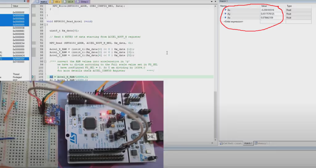
You can see the values of Ax, Ay and Az are being received from the Device. This indicates that the functions we wrote actually works. The STM32 is able to communicate with the slave device (MPU6050) using the I2C.
This STM32 I2C example showed how to configure and communicate via I2C using registers. By avoiding HAL, you get more control and insight into how I2C works on STM32. If you’re exploring more STM32 I2C HAL example code or want a HAL version, let us know in the comments.
STM32 Register based Tutorial Series

STM32F103 Clock Setup using Registers
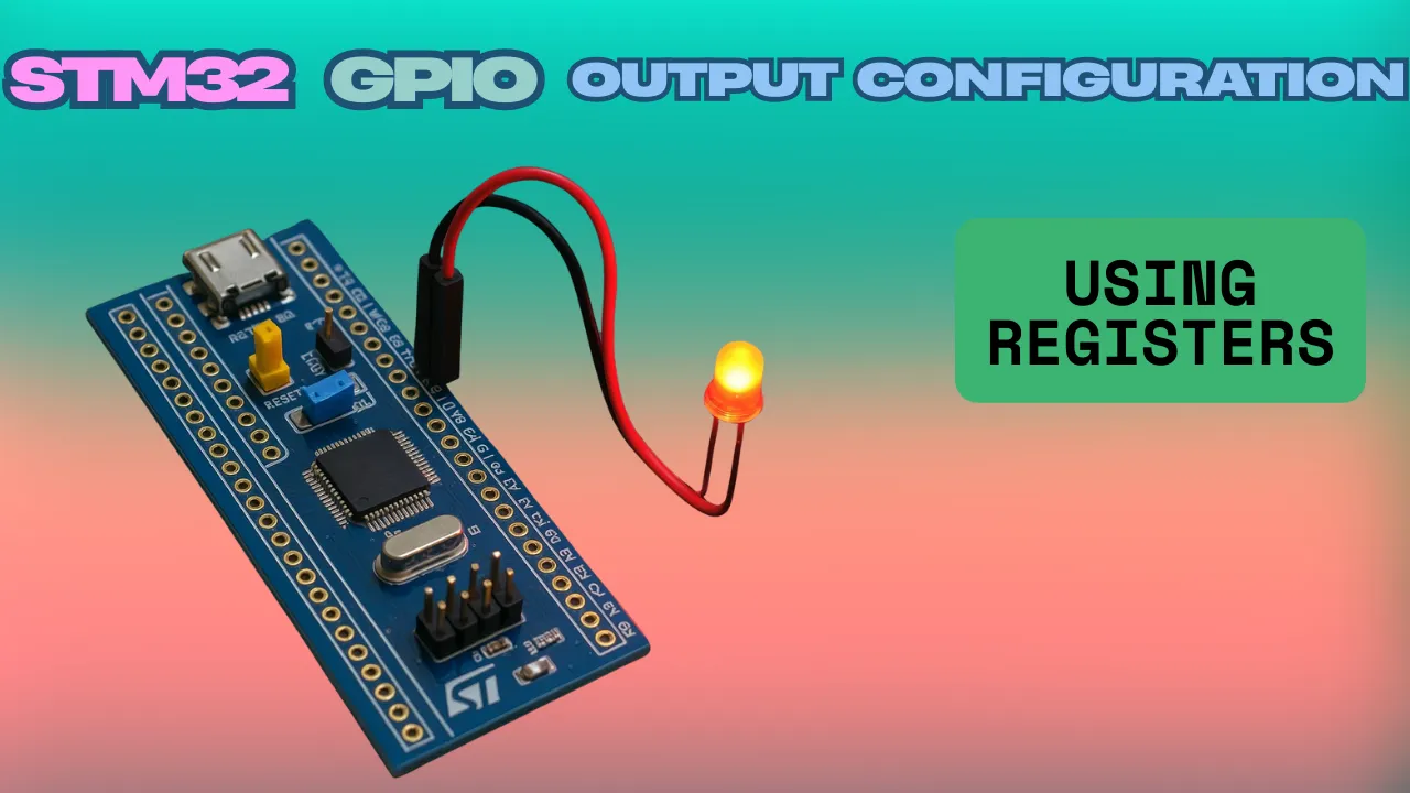
STM32 GPIO Output Example Using Registers | BSRR, MODER, GPIOA Explained
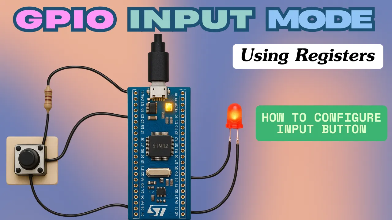
STM32 GPIO Input Configuration – Pin Setup, Pull-Up, and IDR Read
External Interrupt using Registers
STM32 SPI Tutorial Using Registers (Full-Duplex Master with ADXL345)

DMA with ADC using Registers in STM32

How to Setup UART using Registers in STM32
PROJECT DOWNLOAD
Project FAQs


Hi, I applied the same steps when I configured my I2C and I finished it according to my microcontroller. But I am getting an error in the address setting step. It gives an acknowledged error. I am using the STM32F411CExx black pill board and trying to read the temperature value from the MLX90614 temperature sensor.
float MLX90614_TemperatureRead(void){
uint32_t *pI2ControlRegister1 = (uint32_t *) 0x40005400; // I2C_CR1 Register (address offset 0x00)
uint32_t *pI2CStatusRegister1 = (uint32_t *) 0x40005414; // I2C_SR1 Register (address offset 0x14)
uint32_t *pI2CDataRegister = (uint32_t *) 0x40005410; // I2C_DR Register (address offset 0x10)
uint32_t *pI2CStatusRegister2 = (uint32_t *) 0x40005418; // I2C_SR2 Register (address offset 0x18)
uint8_t sensorAddress = 0x5A; // MLX90614 slave address
uint8_t readCommand = 0x07; // Read command ambient temperature
// Start Condition
*pI2ControlRegister1 |= (1 << 10); // Set ACK Bit
*pI2ControlRegister1 |= (1 << 8);
while (!(*pI2CStatusRegister1 & (1 << 0)));
// Send the address
*pI2CDataRegister = (sensorAddress << 1) | 0x00;
while (!(*pI2CStatusRegister1 & (1 << 1))){
if (*pI2CStatusRegister1 & (1 << 10)) { // Check for AF (Acknowledge Failure) flag
*pI2ControlRegister1 |= (1 << 9); // Generate stop condition
return -1; // Return error or handle it accordingly
}
}
// Clear the address flag
(void)*pI2CStatusRegister1;
(void)*pI2CStatusRegister2;
// Write command
*pI2CDataRegister = readCommand;
while (!(*pI2CStatusRegister1 & (1 << 7)));
// Repeat Start Condition
*pI2ControlRegister1 |= (1 << 8);
while (!(*pI2CStatusRegister1 & (1 << 0)));
// Send Register Address for reading
*pI2CDataRegister = (sensorAddress << 1) | 1;
while (!(*pI2CStatusRegister1 & (1 << 1)));
// Clear the address flag
(void)*pI2CStatusRegister1;
(void)*pI2CStatusRegister2;
// Get datas
while (!(*pI2CStatusRegister1 & (1 << 6)));
uint8_t dataLow = *pI2CDataRegister;
*pI2ControlRegister1 |= (1 << 10); // Set ACK Bit
// Last byte operation
*pI2ControlRegister1 &= ~(1 << 10); // Clear ACK Bit
uint8_t dataHigh = *pI2CDataRegister;
*pI2ControlRegister1 |= (1 << 9); // Stop communication
// Combine bytes and converte
uint16_t data = (dataHigh << 8) | dataLow;
float temperature = ((float)data) * 0.02 – 273.15; // Kelvin to Celsius
return temperature;
}
here is my code. I am also learning register manipulation. Is there any error you can see in my code? If the rest of the code is needed I can share the whole code over email.
Looking at the datasheet of MLX90614, it seems like the 0x5A is 7 bit address. So you need to shift it to the left by 1 place, i.e Address = 0x5A<<1.
Yes, I did it but the problem is the same. If you don’t mind me posting the entire code here, I can share the rest of the code here.
hi sir, i followed the same instruction in all of all videos till now, the clock configuration is correct, the UArt worked very well, but im stuck in this one with I2C configuartion , the start is sent correctly and also the addr bit is set when i send the adress,but also TXE bit is set during adress phase which is not correct according to referance manual, so when i get to data writing the BTF bit is not set although the data was written , i dont know where the problem might be ?thanks
The TXE bit is set when the Data Register (DR) is empty. It has nothing to do with address or data. you wait for this bit to set before writing anything (Addr or Data). Check the output on the oscilloscope. There could be a good chance that your slave device is not responding. Also make sure that Pull up registers are connected on both SCL and SDA lines.
I have a question about Clock configuration. Should we finish the first tutorial which is about clock configuration before this tutorial? I am getting an error in address flag so it is about clock mismatch?
Yes obviously. That is why they are numbered.
Thank you for your useful blog. but should be something change when you write into I2C.
at first in multiwrite function
void I2C_WriteMulti (uint8_t *data, uint8_t size)
{
uint8_t i =0;
while (size)
{
while (!(I2C1->SR1 & (1<DR = data[i++]; // send data
size–;
}
while (!(I2C1->SR1 & (1<<2))); // wait for BTF to set
You should wait at the end of process for BTF not after each byte and also in Write Function against use I2C_Write(Reg) you should use code without waiting BTF Flag.
Hello, I have STM32F407 based board. I am trying to read temperature values from BMP280. I run into the issue of ADDR bit not getting set when I send the address bit.
I seem to be stuck in the waiting loop forever after sending the address.
Below is my code snippet.
void send_address(I2C_TypeDef *i2c, unsigned char dev_add)
{
unsigned char regval = 0;
i2c->DR = dev_add;
while(!(i2c->SR1 & I2C_SR1_ADDR))
{
asm(“nop”);
}
regval = i2c->SR2;
}
Will such issue come if I have not connected pull up resistors?
I have a question, i don’t understand why you can use your MPU_Read function to get all accelerometer’s data from reading address ACCEL_XOUT_H 6 time, because I think we need to read all six register ACCEL_XOUT_H, ACCEL_XOUT_L, ACCEL_YOUT_H,… to get all data we need. Sorry for my english
It’s called “burst Read”. The register address gets auto incremented everytime the MCU try to read the data. It’s mentioned in the datasheet somewhere..
Thanks a lot, very usefull. The code works fine but I have a problem with reading multiple bytes. I try with reading two bytes and in debug mode I see that it stops when wait for RxNE to set reading the last byte. I’m trying to read data from LSM9DS1. Thanks for any further explanation.
If it’s waiting for RxNE, means the data is not being transmitted from the slave device. Check the datasheet of the slave, if it supports reading multiple bytes or not
I don’t understand you use two address slave in this function :
void MPU_Read (uint8_t Address, uint8_t Reg, uint8_t *buffer, uint8_t size)
{
	I2C_Start ();
	I2C_Address (Address);
	I2C_Write (Reg);
	I2C_Start ();  // repeated start
	I2C_Read (Address+0x01, buffer, size);
	I2C_Stop ();
}
and i dont’t understand why the Slave Address is (Address+0x01) during the Read function.
Can you explain it to me?
Read address in I2C devices is different from write address.
Any I2C device have the LSB of the Address bit as R/W.
This bit should be 0 for write and 1 for Read.
Please read about peripherals before trying them on MCU, or else things will be confusing
The master can decide to enter Transmitter or Receiver mode depending on the LSB of the
slave address sent.
• In 7-bit addressing mode,
– To enter Transmitter mode, a master sends the slave address with LSB reset.
– To enter Receiver mode, a master sends the slave address with LSB set.
I think the adress of i2c slave when read or write must be or 0x01.
In mode master receiver, i see a small problem in your post. In RM of STM write :
In case a single byte has to be received, the Acknowledge disable and the Stop
condition generation are made just after EV6 (in EV6_1, just after ADDR is cleared)
Bit ACK disable and stop condition generation after EV6 , in EV6_1 – after ADDR clear .
But in your post : the Acknowledge disable is made during EV6 (before ADDR flag is cleared) and the STOP condition generation is made after EV6
I see your point, But it won’t make any difference.
I wrote this according to the F446RE, and in its RM, they have mentioned this
“IN CASE OF THE RECEPTION OF 1 BYTE, THE ACKNOWLEDGE DISABLE MUST BE PERFORMED DURING EV6 EVENT, I.E. BEFORE CLEARING ADDR FLAG.”
I just checked the F103C8 and it’s as per what you said. But this code works with F103 also, so I think it’s okay