Home ▸ STM32 Tutorials ▸
Updated On: September 14, 2025
STM32 GPIO Input Configuration – Read Button State Using Registers (F1 & F4 Series)
This tutorial explains how to configure a STM32 GPIO pin as input using register-level programming, specifically for F1 and F4 series microcontrollers. You’ll learn how to enable GPIO clocks, set pin modes, configure pull-up resistors, and read the input state using the STM32 input data register (IDR). We’ll also demonstrate how a push-button can be used to toggle input states, covering full GPIO input setup for both STM32F103 and STM32F4xx families.
In the previous tutorial, we explored how to configure and use a GPIO pin as an output using register-level programming on an STM32 microcontroller. We saw how to set the pin mode, enable the clock, and then control the pin to turn an LED on or off. That gave us a foundational understanding of GPIO output behavior.
In this tutorial, we’re going to shift our focus to input configuration. Specifically, we’ll learn how to configure a GPIO pin as an input using direct register access. Once the pin is properly configured, we’ll also look at how to read its logic level—whether it’s HIGH or LOW.
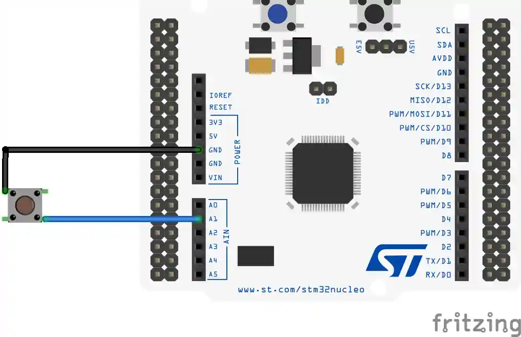
To demonstrate this, I’ll use a simple push-button connected to one of the GPIO pins. When the button is pressed or released, the input pin’s state will change accordingly, and we’ll use this change to trigger some logic in our code—such as incrementing a counter or toggling an LED.
By the end of this tutorial, you’ll understand how to:
- Set up the GPIO pin in input mode,
- Configure the internal pull-up or pull-down resistors,
- And finally, read the pin’s state in real-time.
Configuration for F4 Series
In order to configure the pin in the input mode, we need to follow the steps mentioned below
/************** STEPS TO FOLLOW *****************
1. Enable GPIOA clock
2. Set the PIN PA5 as input
3. Configure the Pull UP / Pull Down mode
************************************************/1. Enable GPIOA clock
The GPIO clock can be enabled in the RCC_AHB1ENR Register

As you can see above, the 0th bit of RCC_AHB1ENR Register enables the clock for the GPIOA. That’s why we need to write a 1 in the 0th position
RCC->AHB1ENR |= (1<<0); // Enable the GPIOA clock2. Set the PIN PA1 as Input
To configure the pin as input, we will modify the GPIOx_MODER Register. This register is responsible for configuring different modes for the GPIO, and in this case we will configure it as the input mode
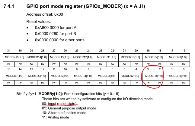
Since I am using pin PA1, I need to modify the pins 2 and 3. This basically works like, if the PIN is ‘y‘, the we need to configure the bits ‘2y’ and ‘2y+1’
Also, in order to set the pin as input, we need to set the bits (3:2) as 0:0. This means that we need to write a ‘0’ in the 2nd and 3rd positions
GPIOA->MODER &= ~((1<<2) | (1<<3)); // pin PA1(bits 3:2) as input (00)3. Configure the Pull UP
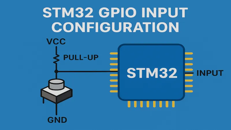
I am going to configure the pin as the Pull-Up pin. The reason for the same is that the button is connected as shown below
When the button will be pressed, the current from the PA1 will sink into the ground, and the PA1 will go LOW.
To configure the Pull UP / Pull DOWN, we need to modify the GPIOx_PUPDR Register
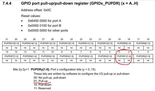
As we need to configure the Pull-UP for the the pin PA1, we need to modify respective bits (3:2). I want to set the Pull-up here, so i need to configure the bits (3:2) as 0:1
GPIOA->PUPDR |= (1<<2); // Pin PA1 (bits 3:2) are 0:1 --> PULL-UPThat’s all for the configuration of the GPIO as input pin.
Configuration for F1 Series
To configure the Pin as the input in F1 series, the steps are shown below
	/*************>>>>>>> STEPS FOLLOWED <<<<<<<<************

	1. Enable GPIO Clock
	2. Set the required Pin in the INPUT Pull-up/ Pull-down Mode
	3. Configure the ODR (1-> Pull UP, 0-> Pull down)

********************************************************/Let’s cover them all one by one
1. Enable the GPIO Clock
Since we are using the pin PA1 as the input, The GPIOA clock can be enabled in the RCC_APB2ENR Register
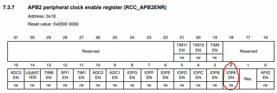
As you can see the 2nd bit of APB2ENR Register controls the GPIOA Clock. So to enable the clock, we will write a ‘1’ in this position
RCC->APB2ENR |= (1<<2); // Enable GPIOA clock2. Set the Pin as INPUT
To control the mode of the pin, we need to modify the Control Register GPIOx_CR.
This Control Register is divided into 2 Registers of 32 bits each i.e CRL(pins 0 to 7) and CRH(pins 8 to 15). Since we are using PA1, we will modify the CRL Register
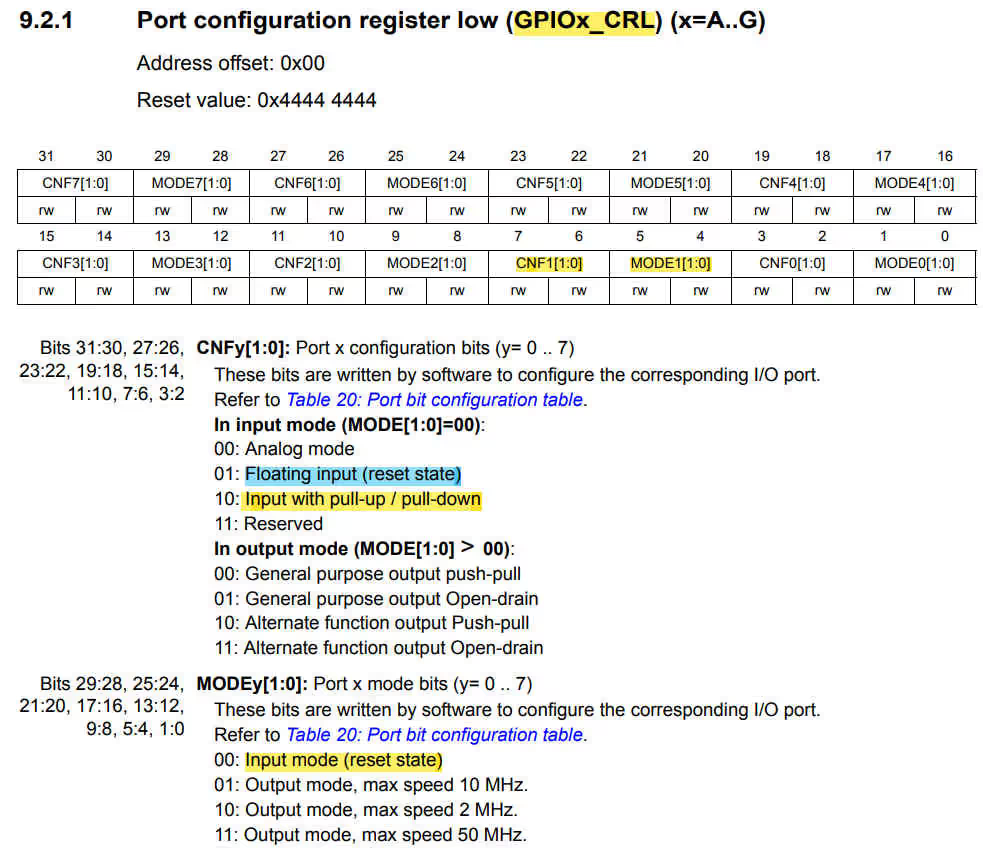
- As you can see above, each pin can be controlled using the 4 bits. For PA1, these bits are 7:6:5:4
- The lower 2 bits can be used to select the mode i.e output or input
- The Higher bits can be used to configure this mode
- Also note that the reset state for the CNF bits is 0:1, so we need to clear the bits before setting a new value there
GPIOA->CRL &= ~(0xf<<4);  // clear bits (7:6:5:4)

GPIOA->CRL |= (8<<4); // Bits (7:6:5:4) = 1:0:0:0 --> PA1 in Input Mode in Pull-up/ Pull-down mode3. Configure the ODR
Here we have selected the input mode with Pull-up/Pull-down mode, but to select the either mode, there is no special register here. This description is provided in the table 20: Port bit configuration table as per the instructions in the picture above.
This table can be seen below
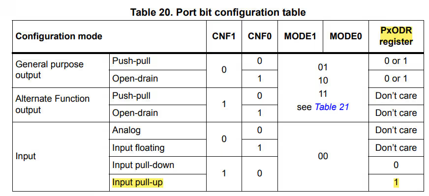
To set the Pull-up register, we need to write a ‘1’ in the Output Data Register (GPIOx_ODR)
GPIOA->ODR |= (1<<1); // --> PA1 is in Pull UP modeThis completes the GPIO Configuration for the F1 Series
Understanding STM32 Pin Configuration Registers
GPIO pins in STM32 are configured using several key registers depending on the MCU series:
- MODER / CRL / CRH: Controls mode (input/output/alternate)
- PUPDR / ODR: Controls pull-up/pull-down configuration
- IDR: Reads current state (HIGH/LOW)
- AHB1ENR / APB2ENR: Enables GPIO peripheral clock
Refer to the STM32 pin diagram and reference manual for correct register mapping and bit positions. This is essential when porting code between F1, F4, and newer STM32 families.
How to Read STM32 GPIO Pin State Using IDR (Input Data Register)
To read the state of the pin, we will check the Input Data Register (IDR)
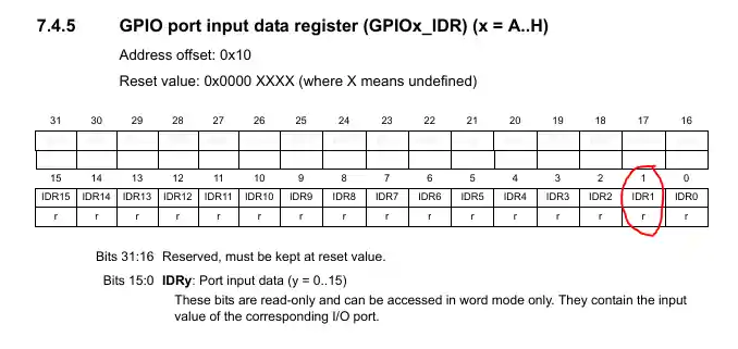
IDR is a read only register. The respective bit either set or reset depending on the state of the PIN.
Now since I am using the Pull-UP for pin PA1 here, the 1st bit of IDR will always be HIGH. When the button is pressed, the current from PA1 will sink into the ground, and the pin will be LOW, and so does the bit 1.
So basically we wait for the 1st bit of the IDR to go LOW. And when it is low, indicating the button has been pressed, we can do the processing.
if (!(GPIOA->IDR &(1<<1)))
{
  while (!(GPIOA->IDR &(1<<1)));
  count++;
}The main CODE
int count = 0;
int main ()
{
SysClockConfig ();
GPIOConfig ();
while (1)
{
if (!(GPIOA->IDR &(1<<1)))
{
  while (!(GPIOA->IDR &(1<<1)));
  count++;
}
}
}Here we check for the bit 1 of the IDR, if it is low, we increment the count variable. So whenever the button is pressed, the count variable will increment.
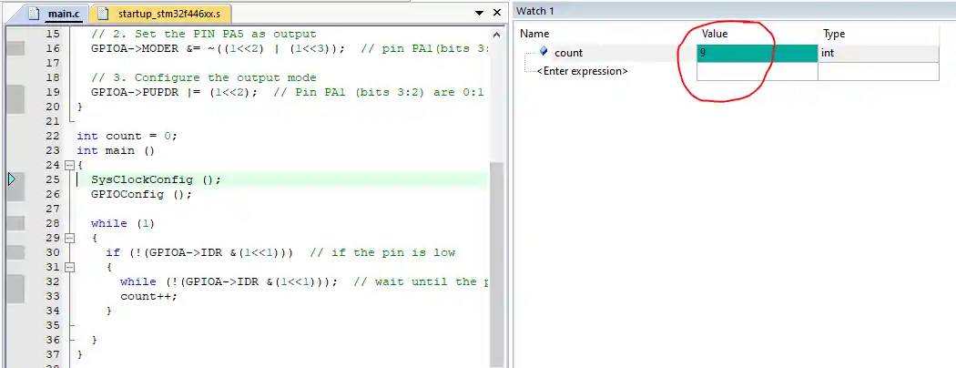
As you can see above, the count variable increments to 9, indicating the button has been pressed 9 times.
Common GPIO Input Use Cases in STM32
Reading GPIO input is often used in embedded projects to:
- Detect button press or switch toggles
- Monitor sensor output (e.g., motion sensors, IR receivers)
- Handle external interrupts or state machines
- Build digital logic input systems (e.g., keypad scanning)
Using direct register access for these tasks gives precise control and fast execution, critical for real-time applications.
With this setup, your STM32 can detect input changes using internal registers, without relying on HAL libraries. Whether you’re building a button interface, digital input handler, or signal monitor, this approach gives full control over GPIO behavior. Understanding STM32 GPIO register configuration is key when optimizing for speed, flash size, or low-level tuning in embedded projects.
STM32 Register based Tutorial Series

STM32F103 Clock Setup using Registers
STM32 GPIO Output Example Using Registers | BSRR, MODER, GPIOA Explained
STM32 I2C Tutorial | Register-Based Configuration with Example Code
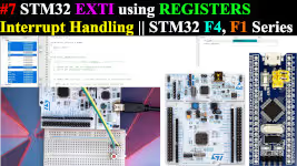
External Interrupt using Registers
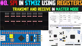
STM32 SPI Tutorial Using Registers (Full-Duplex Master with ADXL345)
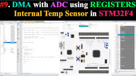
DMA with ADC using Registers in STM32
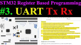
How to Setup UART using Registers in STM32
PROJECT DOWNLOAD
Project FAQs


WHERE IS THE VIDEO TUTORIAL FOR THIS SEGMENT?