Home ▸ STM32 Tutorials ▸
Updated On: September 14, 2025
STM32 GPIO Output Example Using Registers | BSRR, MODER, GPIOA Explained
This STM32 GPIO tutorial explains how to configure GPIO output using STM32 registers. We’ll demonstrate a complete GPIO output example using MODER, OTYPER, OSPEEDR, PUPDR, and BSRR registers. This guide is ideal for understanding how to manipulate the GPIOA port and use BSRR register to toggle pins on STM32F4 microcontrollers. Whether you’re exploring stm32 gpio example projects or learning about gpio registers and stm32 registers, this post covers it all.
In this tutorial, we will learn how to configure a GPIO pin as output on an STM32 microcontroller using direct register programming instead of HAL or STM32CubeMX.
Here’s what you’ll learn step-by-step:
- How to enable the GPIO peripheral clock
- How to set a GPIO pin as output mode
- How to choose between Push-Pull and Open-Drain output types
- How to set the output speed for the pin
- How to configure pull-up or pull-down resistors
- How to write data to the pin using ODR and BSRR registers
- How to toggle an LED using register-level GPIO control
This tutorial gives you a deep understanding of how STM32 GPIO works at the register level and is perfect for those wanting to go beyond HAL and CubeMX for more control and optimization.
You should also take a look at the following:
Why should you Configure the GPIO as output
When we configure a GPIO pin as output on an STM32 microcontroller, we can use it to control other devices.
For example, we can:
- Turn an LED ON or OFF
- Control a buzzer or a relay
- Send signals to other circuits
- Switch motors or sensors using transistors
- Create simple timing signals
By setting up the GPIO output correctly, we make sure the pin works safely and reliably. It’s one of the first things you learn when starting with STM32, and it’s used in almost every embedded project.
Configure the GPIO in Output Mode
Let’s start with the simplest, and the most used one i.e the output mode. I will use Pin PA5 as the output pin. Following are the steps required to configure the pin as the output Pin.
/************** STEPS TO FOLLOW *****************
1. Enable GPIOA clock
2. Set the PIN PA5 as output
3. Configure the output mode i.e state, speed, and pull
************************************************/1. Enable GPIOA Clock
The GPIO clock can be enabled in the RCC_AHB1ENR Register

As you can see above, the 0th bit of RCC_AHB1ENR Register enables the clock for the GPIOA. That’s why we need to write a 1 in the 0th position
RCC->AHB1ENR |= (1<<0); // Enable the GPIOA clock2. Set the PIN PA5 as output
To configure the pin as output, we will modify the GPIOx_MODER Register. This register is responsible for configuring different modes for the GPIO and in this case, we will configure it as the output mode
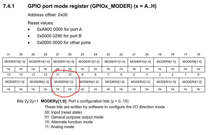
Since I am using pin PA5, I need to modify the pins 10 and 11. This basically works like, if the PIN is ‘y‘, the we need to configure the bits ‘2y’ and ‘2y+1’
Also, in order to set the pin as output, we need to set the bits (11:10) as 0:1. This means that we need to write a ‘1’ in the 10th position
GPIOA->MODER |= (1<<10); // pin PA5(bits 11:10) as Output (01)3. Configure the output mode i.e Output type, speed, and pull
The output type can be configured in the GPIOx_OTYPER Register.
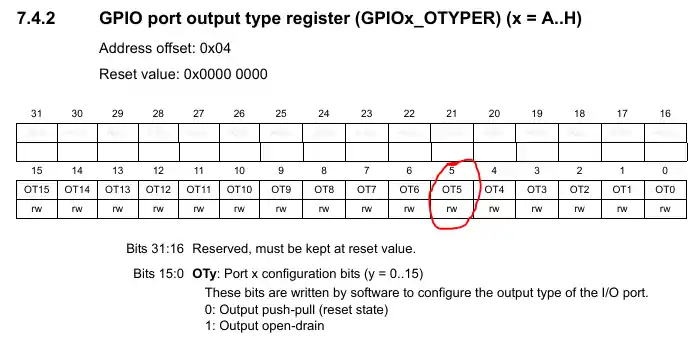
In the simplest words, the difference between the Push-Pull and open Drain can be understood as follows
If you choose open drain, then the output pin can either be LOW (Gnd) or it can be floating, while if you choose Push-Pull, the the output pin can be HIGH or LOW
Since I want to blink the LED on pin PA5, i will choose the push-pull type output, and to do so, I need to write a ‘0‘ in the 5th position
GPIOA->OTYPER &= ~(1<<5); // bit 5=0 --> Output push pullNext, The output speed can be configured in the GPIOx_OSPEEDR Register
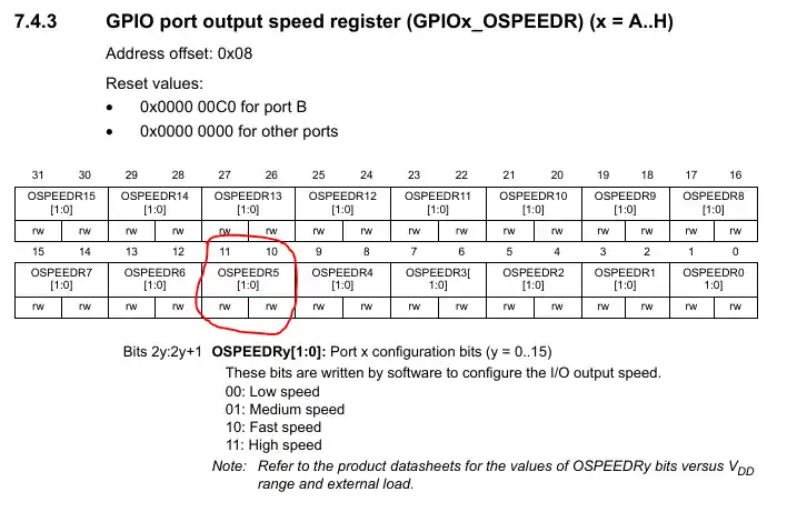
Here you can select different Speeds for the Output Pin, as per your requirement. GPIO speed controls the rate at which a signal can change between low/high values (the “rise time” and “fall time”).
I want the speed not too high and not too low, so I will choose the Fast speed. To do so, I need to write 1:0 to bits (11:10)
GPIOA->OSPEEDR |= (1<<11); // Pin PA5 (bits 11:10) as Fast Speed (1:0)Now the final step is to configure the pull-up/pull-down (GPIOx_PUPDR) register.
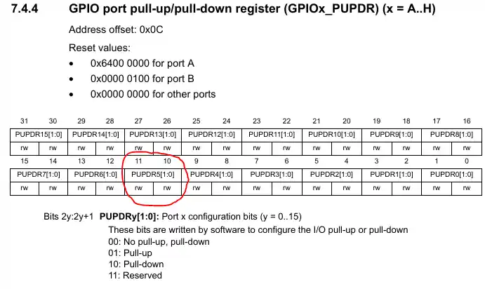
Here we can Pull-up the pin to Vcc or Pull-down to ground, as per the requirement. Since I am using the pin to blink LED, i will not use the Pull-up or Pull-down. I will set the bits (11:10) as 0
GPIOA->PUPDR &= ~((1<<10) | (1<<11)); // Pin PA5 (bits 11:10) are 0:0 --> no pull up or pulldownThis completes the configuration for the output mode. Now we will see how to set or reset the pin so that we can toggle the LED attached to it
How to Set/Reset the Pin
After setting a GPIO pin as output, we can use it to turn things ON or OFF. In STM32, this is done by writing to special registers. We can use the BSRR register to quickly set or reset the pin, or the ODR register to control the pin value directly.
This helps us control devices like LEDs, buzzers, or relays from our code.
Control Output Pin Using BSRR
To set or reset an individual pin, we need to modify the GPIOx_BSRR Register
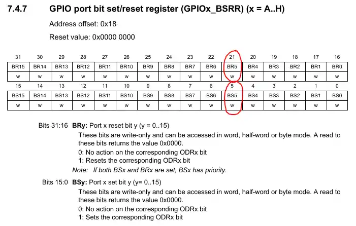
BSRR is a 32 bit Register. The lower 16 bits (bit 0 – bit 15) are responsible to set a bit, and the higher 16 bits (bit 16 – bit 31) are responsible to reset a bit
As I have connected the LED to PA5, in order to set it (turn the LED ON), I will write a 1 to bit 5
GPIOA->BSRR |= (1<<5); // Set the Pin PA5And to reset the pin PA5 (turn the LED OFF), I will write a 1 to the bit 21
GPIOA->BSRR |= (1<<21); // Reset the Pin PA5Control Output Pin Using ODR
Output Data Register (ODR) can also be used to Set/Reset an individual Pin or the entire Port.
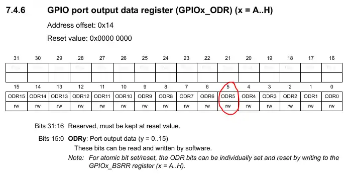
In order to Set a pin, we can directly write a ‘1’ to the respective bit, and in order to Reset it, write a ‘0’ in the respective bit
GPIOA->ODR |= 1<<5; // Set the Pin PA5

GPIOA->ODR &= ~(1<<5); // Reset the Pin PA5To set the entire PORT HIGH, we can write 0xFFF to the ODR
GPIOA->ODR = 0xFFF;  // Set the PORTA HIGH

GPIOA->ODR = 0x00; // Reset the PORTAThis will toggle all the Pins of PORTA (PA0 – PA15).
STM32 GPIOA Register-Level LED Blinking Example
Now let’s combine our understanding of MODER, BSRR register, and other GPIO registers to toggle PA5 (connected to an LED). This GPIOA example uses register-level control for precise and low-level pin manipulation.
void Delay (uint32_t time)
{
	while (time--);
}

int main (void)
{
	SysClockConfig ();
	GPIOConfig ();

	while (1)
	{
		GPIOA->BSRR |= (1<<5); // Set the Pin PA5
//		GPIOA->ODR = 1<<5;
		Delay (10000000);  // random delay
		GPIOA->BSRR |= (1<<5) <<16;  // Clear the Pin PA5
//		GPIOA->ODR &= ~(1<<5);
		Delay (10000000);  // random delay
	}

}This code turns an LED connected to PA5 ON and OFF with a delay in between.
GPIOA->BSRR |= (1<<5);sets (turns ON) the PA5 pinGPIOA->BSRR |= (1<<5)<<16;resets (turns OFF) the PA5 pin- The
Delay()function creates a simple wait loop - This ON/OFF cycle repeats forever in the
while(1)loop
This STM32 GPIO output example shows how to configure GPIOA using registers. We used the BSRR register to toggle pins efficiently and explained how each GPIO register like MODER, OTYPER, and OSPEEDR works. If you’re looking for more stm32 gpio register or bsrr register examples, check out the related tutorials.
STM32 Register based Tutorial Series

STM32F103 Clock Setup using Registers
STM32 GPIO Input Configuration – Pin Setup, Pull-Up, and IDR Read
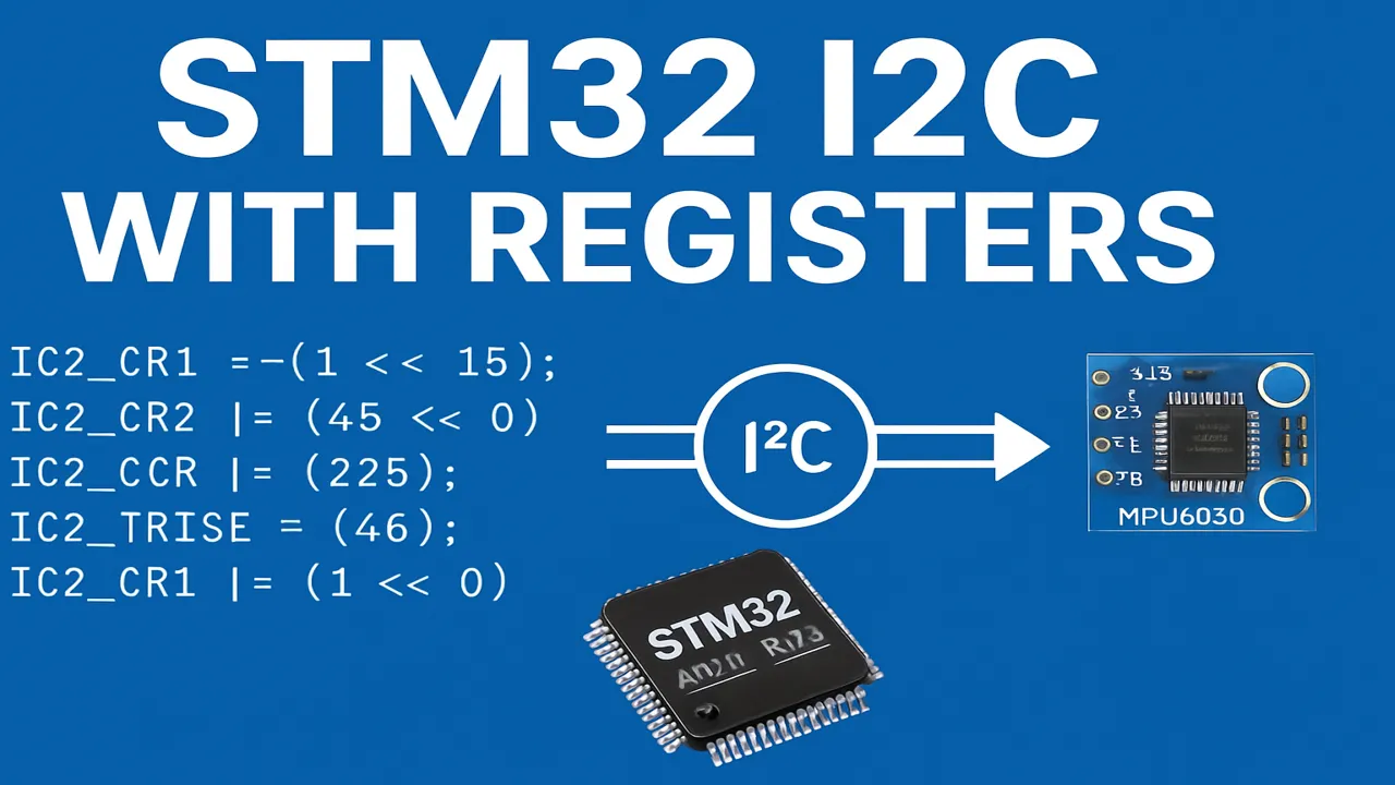
STM32 I2C Tutorial | Register-Based Configuration with Example Code
External Interrupt using Registers
STM32 SPI Tutorial Using Registers (Full-Duplex Master with ADXL345)

DMA with ADC using Registers in STM32
How to Setup UART using Registers in STM32
PROJECT DOWNLOAD
Project FAQs


could somebody please help me with this:
i have done the clock configuration and Timer for delay and also the GPIO configuration: the LED does blink with instead of 1s it takes like 4s , i have done a lot of research to find out where the problem might be , but found nothing. here ist my code :
void Clock_Config(void)
{
RCC->CR |=(RCC_CR_HSEON);
while(!((RCC->CR) & (RCC_CR_HSERDY)));
RCC->APB1ENR |= (1<CR |= 1<ACR |= (1<<8)|(1<<9)|(1<<10)|(2<CFGR|=RCC_CFGR_HPRE_DIV1;
RCC->CFGR |= RCC_CFGR_PPRE1_DIV4;
RCC->CFGR |= RCC_CFGR_PPRE2_DIV2;
RCC->PLLCFGR |= (0<<16)|(4<<0)|(180<CR |=(RCC_CR_PLLON);
while(!((RCC->CR) & (RCC_CR_PLLRDY)));
RCC->CFGR |=(RCC_CFGR_SW_PLL);
while ((RCC->CFGR & RCC_CFGR_SWS) != RCC_CFGR_SWS_PLL);
}
void Timer_Config(void)
{
RCC->APB2ENR|=(1<PSC=180-1;
TIM1->ARR=0xffff;
TIM1->CR1|=1<SR)& (1<CNT=0;
while (TIM1->CNT<µs);
}
void Delay_ms (int ms)
{
for (uint16_t counter=0;counterAHB1ENR |=(1<MODER|=(1<<26)|(1<OTYPER&=~(0<<13)|~(1<OSPEEDR |=(2<<26) | (2<PUPDR&=~((1<<26) | (1<<28));
}.
You missed the entire point of the BSRR register. It’s purpose is to allow users to modify GPO specific to their context in an atomic call. No issues of being interrupted between the read and write and corruption of state. You don’t have to care about the previous state and can simply write the register with the bits you wish to affect, any zero in the bitfield will result in no changes.
seems the | is not necessary. check the HAL_GPIO_WritePin(), they don’t use |. also tested with actual device and oscilloscope, without |, it works well
GPIOA->BSRR = PROBE_Pin;
GPIOA->BSRR = (uint32_t) PROBE_Pin << 16u;
I mean….set another PIN A first before the main while(1), then keep calling the BSRR set and reset in main while(1), check PIN A ‘s value, it remains the same.
Thanks for this tutorial. It’s really helpful to understand registers. However, I don’t get success applying this example to the STM32H743ZIT6U, board NUCLEO-H743ZI2.
I’m trying to blink the LED1 (PB0). My code is as follows.
#include “stm32h7xx.h”
int main(void)
{
RCC->AHB4ENR |= (1<<1); // enable the clock to GPIOB
GPIOB->MODER |= (1<<0); // set pins to be general purpose output
GPIOB->OTYPER &= ~(1<<0); // push pull
GPIOB->OSPEEDR |= (1<<1);
GPIOB->PUPDR &= ~((1<<0) | (1<<1));
for (;;) {
GPIOB->BSRR |= (1<<0); // or GPIOB->ODR = 0xFFF;
for(int i = 0; i < 1000000; i++);
GPIOB->BSRR |= (1<<16); // or GPIOB->ODR = 0x00;
for(int i = 0; i < 1000000; i++);
}
return 0;
}
Please, could you have a look at it?
For the STM32H743, the default value for GPIOx->MODER = 11
To set the output, firstly we have to clean up these to bits. Add GPIOB->MODER &= ~((1<<0) | (1<<1)); before GPIOB->MODER |= (1<<0);
The compiler removes your delay code because it does nothing.
for(int i = 0; i < 1000000; i++);
if you something like asm("") inside, it would not be erased.
You should not be setting bits in the BSRR using an OR command. The BSRR register is meant to be atomic and therefore use EQUALS to set and reset bits. It should not use Read-Modify-Write command such as OR/AND/XOR etc. If you want to use these then use them on the ODR.