Home ▸ STM32 Tutorials ▸
Updated On: September 14, 2025
DMA with ADC using Registers in STM32
This is yet another tutorial in the Register base programming series, and today we will see how to use DMA in STM32. Here I will use the ADC along with DMA, without any interrupt.
I am choosing ADC for this tutorial because the conversion of these values will take place in the background, without affecting the CPU, and whenever we need the ADC value for some processing, we can just take it from the buffer.
This way we will always get the latest value from the ADC.
Let’s start with ADC Configuration
As much as the explanation remains same across most of the STM32 devices, some might require additional setup. The BluePill code can be accessed at https://github.com/controllerstech/STM32/tree/master/F103_RegisterBased/ADC%20with%20DMA
VIDEO TUTORIAL
You can check the video to see the complete explanation and working of this project.
ADC CONFIGURATION
Below are the Steps to configure the ADC in the DMA mode.
/************** STEPS TO FOLLOW *****************

1. Enable ADC and GPIO clock
2. Set the prescalar in the Common Control Register (CCR)
3. Set the Scan Mode and Resolution in the Control Register 1 (CR1)
4. Set the Continuous Conversion, EOC, and Data Alignment in Control Reg 2 (CR2)
5. Set the Sampling Time for the channels in ADC_SMPRx
6. Set the Regular channel sequence length in ADC_SQR1
7. Set the Respective GPIO PINs in the Analog Mode

************************************************/Let’s cover them all one by one
1. Enable ADC and GPIO clock
I am using multiple channels for ADC1 in this tutorial. To be precise, I am going to use channel 1 and channel 4.
Channel is is connected to the PA1 and channel 4 is connected to PA4
So I would need to enable the GPIOA clock here.
//1. Enable ADC and GPIO clock
	RCC->APB2ENR |= (1<<8);  // enable ADC1 clock
RCC->AHB1ENR |= (1<<0); // enable GPIOA clock2. Set the prescalar in the Common Control Register (CCR)
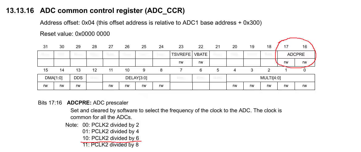
In this case, the ADC1 is connected to the APB2 Peripheral clock, which is running at it’s maximum speed of 90 MHz
We will use the prescalar to bring the ADC1 clock down.
The Prescalar selection can be done in the CCR Register. The important point to note here is that we can only choose amongst the predefined Prescalar values. This is shown in the figure below
//2. Set the prescalar in the Common Control Register (CCR)
ADC->CCR |= 2<<16; // PCLK2 divide by 6.... ADC_CLK = 90/6 = 15MHzHere I have used the presclalar of 6, so the ADC clock = 90/6 = 15 MHz.
3. Set the Scan Mode and Resolution in the Control Register 1 (CR1)
Now we will modify the Control Register 1 (CR1). Here we will set up the scan mode and the Resolution for the ADC1.
Scan mode must be set, if you are using more than 1 channel for the ADC.
Resolution defines the Resolution of the ADC. In STM32F4, this can vary between 6-Bit, 8-Bit, 10-Bit or 12-Bit.
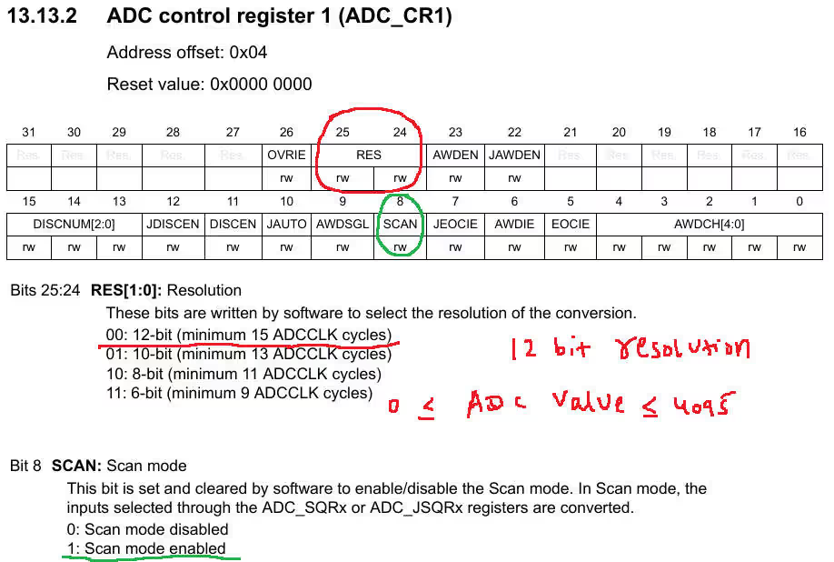
Here choosing the Resolution of 12 bit means, the ADC values will vary between 0 to 4095.
//3. Set the Scan Mode and Resolution in the Control Register 1 (CR1)
ADC1->CR1 = (1<<8);    // SCAN mode enabled
ADC1->CR1 &= ~(1<<24); // 12 bit RES4. Set the Continuous Conversion, EOC, DMA and Data Alignment in Control Reg 2 (CR2)
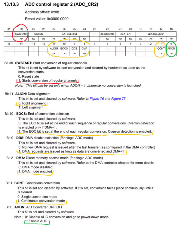
We have to modify the Control Register 2 in order to set all the things mentioned here.
- Continuous Conversion specifies whether we want to convert the ADC values continuously, or should it stop after one conversion only.
- EOC is End Of Conversion specifies whether the EOC Flag should set after each conversion, or at the end of all the conversions.
- DMA specifies whether we want to use DMA for ADC.
- Data Alignment specifies whether the 12 bit data should be Right Aligned or Left Aligned in a 16 bit Register.
//4. Set the Continuous Conversion, EOC, and Data Alignment in Control Reg 2 (CR2)
ADC1->CR2 = (1<<1);     // enable continuous conversion mode
ADC1->CR2 |= (1<<10);    // EOC after each conversion
ADC1->CR2 &= ~(1<<11);   // Data Alignment RIGHT
// Enable DMA for ADC
ADC1->CR2 |= (1<<8);
// Enable Continuous Request
ADC1->CR2 |= (1<<9);- Here I am choosing the Continuous Mode, so that the conversion would not stop.
- EOC will be set after each conversion
- Data Alignment will be to the right
- Enable the DMA mode, as we will be using DMA in this tutorial
- The DMA requests will be continuous, and they will only disable, if the DMA itself is disabled
5. Set the Sampling Time for the channels
Each channel can be set with a different sampling time/Frequency. This can be controlled in the ADC sample time register
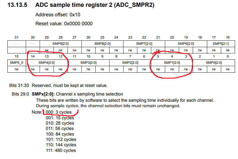
There are 2 sample Registers SMPR1 and SMPR2. Since I am using channel 1 and channel 4, I have to use SMPR2.
For this demonstration, we don’t need any specific timing for the ADC, and that’s why we can choose any sampling cycle from above.
I am going to choose the 3 cycles from here. For more information on how to find sampling time/frequency, check out ADC conversion Time/Frequency Calculation in STM32
//5. Set the Sampling Time for the channels
ADC1->SMPR2 &= ~((7<<3) | (7<<12)); // Sampling time of 3 cycles for channel 1 and channel 46. Set the Regular channel sequence length
Now we will set the number of channels that we are concerting. This can be done in the ADC Sequence Register 1 (ADC_SQR1)
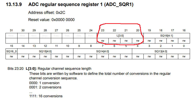
Here L can be used to set the number of channels. As you can see in the picture above, we can set the number of channels between 1 to 16. A single ADC is capable of converting 16 channels at once.
Since we are converting 2 channels, we would write 1 in the 20th position.
//6. Set the Regular channel sequence length in ADC_SQR1
ADC1->SQR1 |= (2<<20); // SQR1_L =2 for 3 conversionsWe also need to set the sequence for the conversion. Like which channel will be converted first, which will be converted second, and so on. There are 3 sequence registers, and based on how many channels you want to convert, you can use these registers.
Here we are converting 2 channels only, so we will need to configure the sequence register 3.
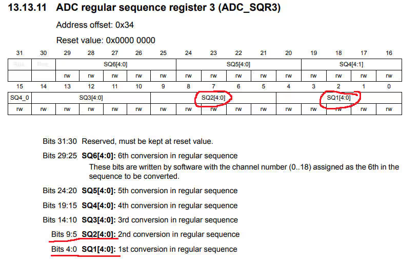
The first 2 sequences, SEQ1 and SEQ2, will be set for the channel 1 and channel 4 respectively. To do this all we have to do is, write the channel number to the respective sequence.
// Channel Sequence
ADC1->SQR3 |= (1<<0);  // SEQ1 for Channel 1
ADC1->SQR3 |= (4<<5);  // SEQ2 for CHannel 4
ADC1->SQR3 |= (18<<10); // SEQ3 for CHannel 18Above I have used the examples of 3 channels, just to show how it’s done. the third channel is just for the demonstration purpose.
7. Set the Respective GPIO PINs in the Analog Mode
Now it’s time to configure the Pins. To use the ADC, we must set the Pins in the Analog mode.
We have to go to the GPIO Registers now.
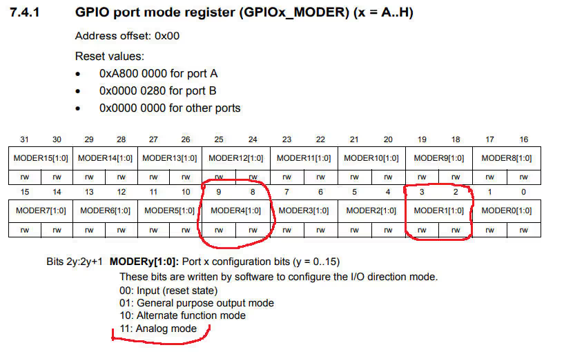
GPIO Mode Register can be used to modify the Pin Modes. Here we need to set the Analog mode to the Pins PA1 and PA4, and that’s why we will modify the MODER1 (Bits 2 and 3) and MODER4 (Bits 8 and 9).
//7. Set the Respective GPIO PINs in the Analog Mode
GPIOA->MODER |= (3<<2);  // analog mode for PA 1
GPIOA->MODER |= (3<<8); // analog mode for PA 4Enable the ADC
Once the ADC configuration is complete, we will enable the ADC. This is important to enable it in the end because we can not configure certain things while the ADC is enabled.
We will again modify the Control Register 2 for this
As shown in the picture above that the 0th Bit of CR2 enabled the ADC. So we will set this bit.
ADC1->CR2 |= 1<<0;   // ADON =1 enable ADC1

uint32_t delay = 10000;
while (delay--);Start the ADC
After setting everything, ADC, DMA etc, we will start the ADC to start the conversion of the selected channels.
This will again require to modify the Control Register 2.
As shown in the picture above, the 30th Bit of the CR2 is the SWSTART Bit. This Bit starts the conversion of the Regular Channels.
We have to also make sure that the status Register is reset, or else the conversion will not start.
ADC1->SR = 0;        // clear the status register

ADC1->CR2 |= (1<<30); // start the conversionThis is it for the ADC Related setup. Now we will configure the DMA.
DMA Configuration
DMA Configuration is split into 2 parts.
First we will initialize the DMA. This part will remain common for anything that we are going to use the DMA with.
and after that we will configure the DMA. This part will change based on some parameters.
Initialize the DMA
Here are the Steps for Initializing the DMA
/************** STEPS TO FOLLOW *****************

1. Enable DMA clock
2. Configure the Configuration Register

************************************************/1. Enable the DMA Clock
F446RE have 2 DMAs, DMA1 and DMA2. I am using DMA2 here, and I will explain the reason in a while. The DMA2 clock can be enabled in the RCC AHB1ENR Register
// Enable the DMA2 Clock
RCC->AHB1ENR |= (1<<22); // DMA2EN = 12. Configure the Configuration Register
There are a lot of things to be configured in the configuration Register. These are The Data Direction, The Circular Mode, Peripheral and memory increment modes, The data size, channel selection, etc.
Before doing any of this, we need to find out which DMA and what channel/stream that we are going to use. This information is provided in the DMA section of the reference manual itself.
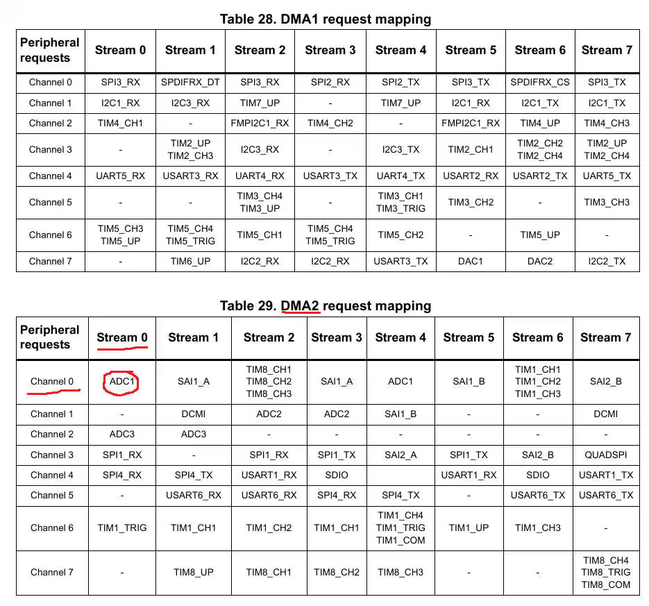
As shown in the picture above, the ADC1 uses DMA2, Channel 0, Stream 0. We will keep this in mind while configuring the DMA.
// Select the Data Direction
DMA2_Stream0->CR &= ~(3<<6);  // Peripheral to memory

// Select Circular mode
DMA2_Stream0->CR |= (1<<8);  // CIRC = 1

// Enable Memory Address Increment
DMA2_Stream0->CR |= (1<<10);  // MINC = 1;

// Set the size for data
DMA2_Stream0->CR |= (1<<11)|(1<<13);  // PSIZE = 01, MSIZE = 01, 16 bit data

// Select channel for the stream
DMA2_Stream0->CR &= ~(7<<25); // Channel 0 selectedBelow is the Picture of the DMA CONFIGURATION REGISTER
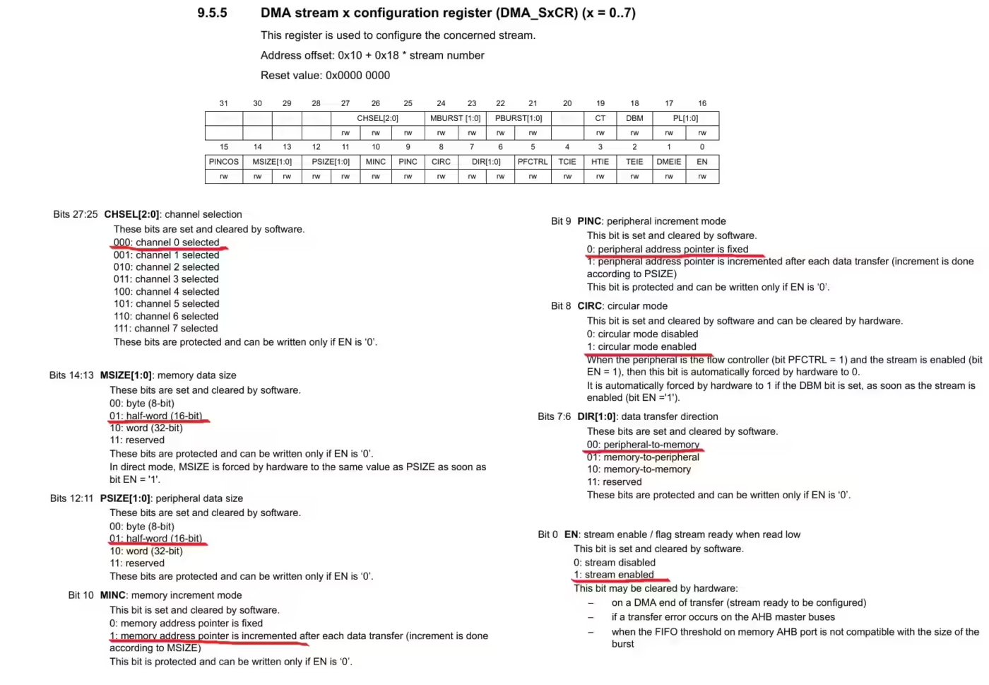
- Since we are transferring the data from ADC (Peripheral) to Buffer (Memory), the data direction needs to be Peripheral to Memory.
- CIRC Bit must be one, since we are using the circular mode for the DMA. This will make the DMA to continuously request the converted data from the ADC.
- We will enable the Memory Increment. This will increment the address of the memory after the transfer of each data.
- Peripheral Increment must be disabled, because we always want to copy the data from the Data Register of the ADC.
- The data Size is selected as 16 bit wide. This is because I am using ADC in 12 bit mode here, and that’s why the data size should be more than this.
- And at last we will select the channel for the DMA. I am using Channel 0, because that’s where the ADC1 is connected to.
Note:- If you read the Description below every Bit, It is mentioned that we can only modify them when the Enable Bit is 0. This is the Reason we haven’t enabled the ENABLE Bit yet. We will enable it after everything is setup in the DMA.
This completes the initialization of the DMA, and this will pretty much remains same for all the peripheral we are reading the data from.
CONFIGURE THE DMA
The configuration depends on things like which peripheral are we using, where in the memory are we saving the data, and how much is the data size. This changes according to your setup.
Below are the steps to configure the DMA
/************** STEPS TO FOLLOW *****************

1. Set the Data Size in the NDTR Register
2. Set the Peripheral Address and the Memory Address
3. Enable the DMA Stream

************************************************/DMA2_Stream0->NDTR = size; // Set the size of the transfer
DMA2_Stream0->PAR = srcAdd; // Source address is peripheral address
DMA2_Stream0->M0AR = destAdd; // Destination Address is memory address
// Enable the DMA Stream
DMA2_Stream0->CR |= (1<<0); // EN =1- Here we will first set the Size in the NDTR Register. This is basically the number of data items, that we want transfer using the DMA.
After each transfer, this value decreases. And once it reaches 0, the data transfer will stop.
In case of circular mode, it never reaches 0, as it gets updated again. - PAR Register is used to store the address of the Peripheral Register, which will be involved in the data transfer. In our case it’s the source, so we will pass the source address here. This you will see in a while
- M0AR Register is used to store the address of the Memory, which will be involved in the data transfer. In our case it’s the Destination, so we will pass the destination address here.
- After all the setup is finished, we will finally enable the DMA.
The Main Function
int main ()
{
	SysClockConfig ();
	TIM6Config ();
	ADC_Init ();
	ADC_Enable ();
	DMA_Init ();
	DMA_Config ((uint32_t ) &ADC1->DR, (uint32_t) RxData, 2);
	ADC_Start ();
	while (1){}
}- Here we will initialize the ADC and DMA first.
- In the DMA Configuration, the source address the the address of the data register of ADC1
The Destination address is the address of the RxData buffer. - Since we are converting 2 channels, the size (NDTR Value) will be 2.
This conversion will keep happening in the background, and we will always get the latest values in the buffer. We can use these values at any point in our program to do the further calculations.
STM32 Register based Tutorial Series

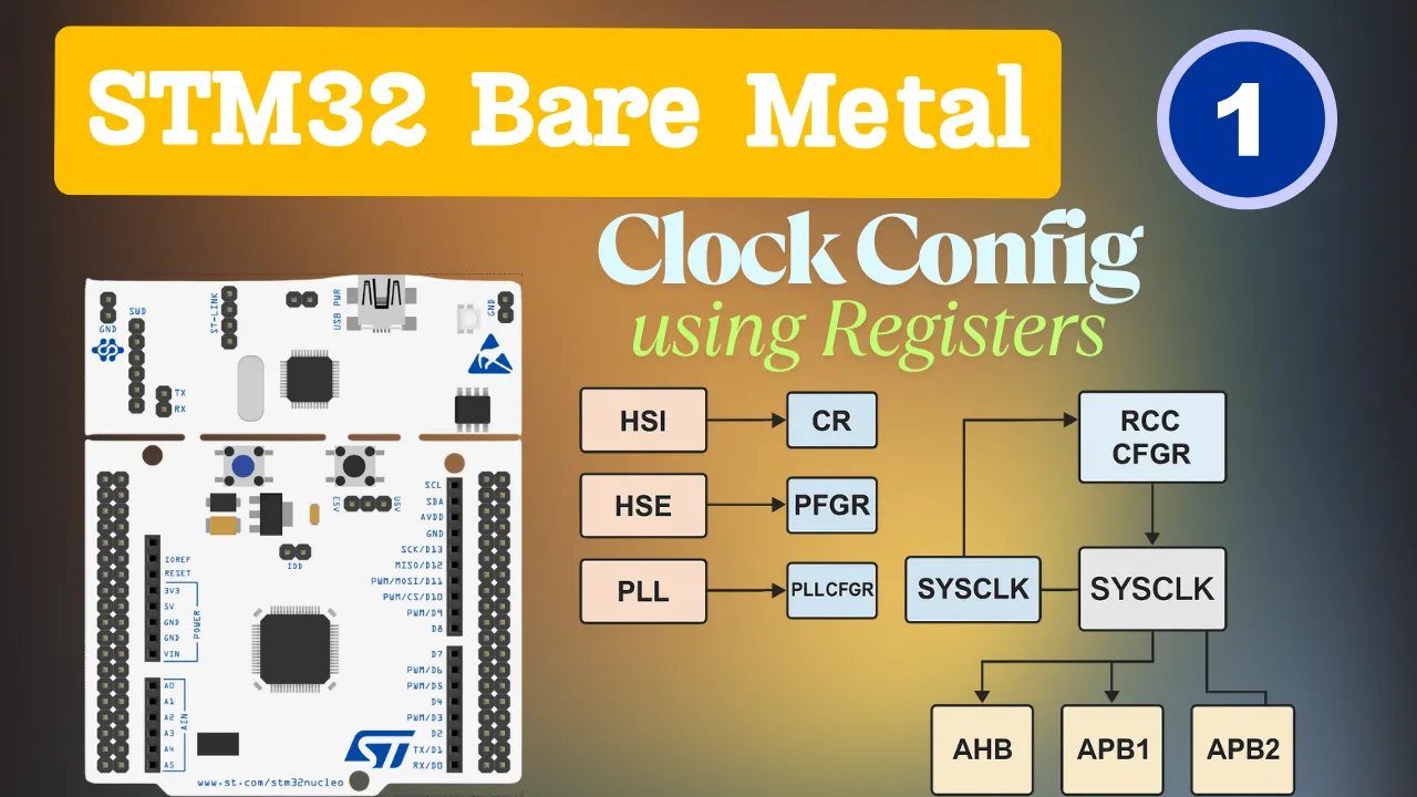
STM32F103 Clock Setup using Registers
STM32 GPIO Output Example Using Registers | BSRR, MODER, GPIOA Explained
STM32 GPIO Input Configuration – Pin Setup, Pull-Up, and IDR Read
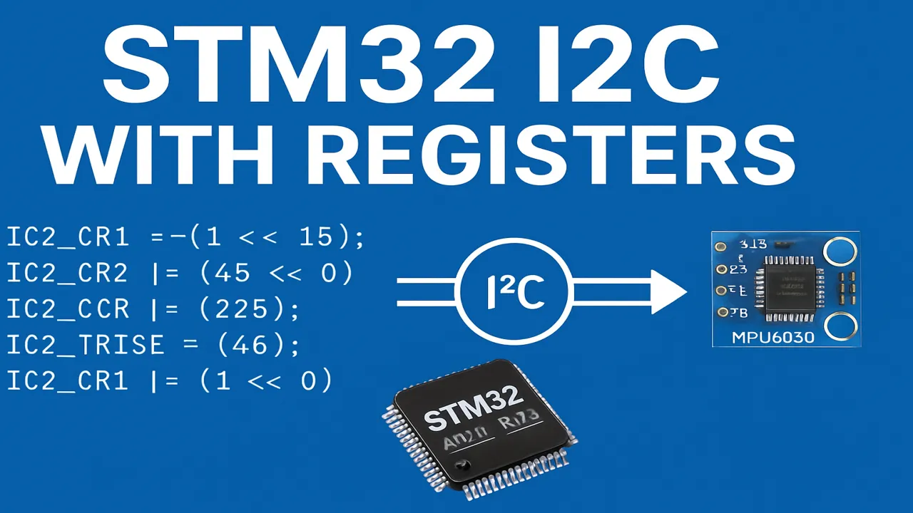
STM32 I2C Tutorial | Register-Based Configuration with Example Code
External Interrupt using Registers
STM32 SPI Tutorial Using Registers (Full-Duplex Master with ADXL345)

How to Setup UART using Registers in STM32

Subscribe
Login
0 Comments
Newest
