Home ▸ STM32 Tutorials ▸
Updated On: September 14, 2025
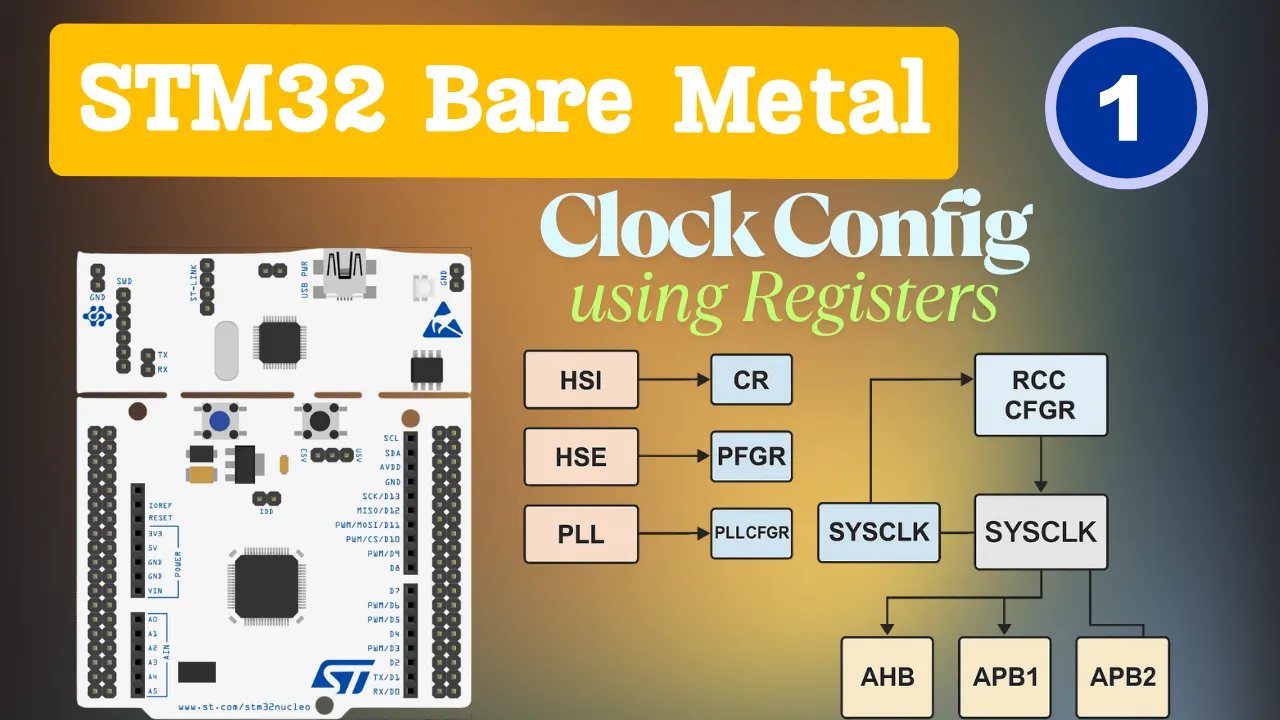
STM32F103 Clock Setup using Registers
This tutorial will cover Clock setup, Timer Setup for Delay, and GPIO configuration for STM32F103C8 (BluePill) using the Register based programming. I will cover all the steps, and the link to download the code is at the end of this post.
Before starting the main setup, Let’s see the clock setup that we will be using in this tutorial.
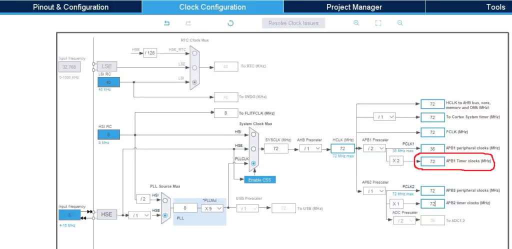
As you can see above, the system will run at 72 MHz. Also take note of the APB1, and APB2 clocks, since they will be used in the timer setup
VIDEO TUTORIAL
You can check the video to see the complete explanation and working of this project.
MAIN CLOCK SETUP
This part is very simple in BluePill compared to STM32F4 devices. The reason is that the function to set up the clock is predefined in the core files that we include in our project. Check the code below
void SystemInit (void)
{
  /* Reset the RCC clock configuration to the default reset state(for debug purpose) */
  /* Set HSION bit */
  RCC->CR |= (uint32_t)0x00000001;

  /* Reset SW, HPRE, PPRE1, PPRE2, ADCPRE and MCO bits */
#ifndef STM32F10X_CL
  RCC->CFGR &= (uint32_t)0xF8FF0000;
#else
  RCC->CFGR &= (uint32_t)0xF0FF0000;
#endif /* STM32F10X_CL */

  /* Reset HSEON, CSSON and PLLON bits */
  RCC->CR &= (uint32_t)0xFEF6FFFF;

  /* Reset HSEBYP bit */
  RCC->CR &= (uint32_t)0xFFFBFFFF;

  /* Reset PLLSRC, PLLXTPRE, PLLMUL and USBPRE/OTGFSPRE bits */
  RCC->CFGR &= (uint32_t)0xFF80FFFF;

#ifdef STM32F10X_CL
  /* Reset PLL2ON and PLL3ON bits */
  RCC->CR &= (uint32_t)0xEBFFFFFF;

  /* Disable all interrupts and clear pending bits  */
  RCC->CIR = 0x00FF0000;

  /* Reset CFGR2 register */
  RCC->CFGR2 = 0x00000000;
#elif defined (STM32F10X_LD_VL) || defined (STM32F10X_MD_VL) || (defined STM32F10X_HD_VL)
  /* Disable all interrupts and clear pending bits  */
  RCC->CIR = 0x009F0000;

  /* Reset CFGR2 register */
  RCC->CFGR2 = 0x00000000;
#else
  /* Disable all interrupts and clear pending bits  */
  RCC->CIR = 0x009F0000;
#endif /* STM32F10X_CL */

#if defined (STM32F10X_HD) || (defined STM32F10X_XL) || (defined STM32F10X_HD_VL)
  #ifdef DATA_IN_ExtSRAM
    SystemInit_ExtMemCtl();
  #endif /* DATA_IN_ExtSRAM */
#endif

  /* Configure the System clock frequency, HCLK, PCLK2 and PCLK1 prescalers */
  /* Configure the Flash Latency cycles and enable prefetch buffer */
  SetSysClock();

#ifdef VECT_TAB_SRAM
  SCB->VTOR = SRAM_BASE | VECT_TAB_OFFSET; /* Vector Table Relocation in Internal SRAM. */
#else
  SCB->VTOR = FLASH_BASE | VECT_TAB_OFFSET; /* Vector Table Relocation in Internal FLASH. */
#endif
}This function SystemInit() is already present in system_stm32f10x.c file. All we need to do is call it in our main function and the clock setup will be complete
If you take a look at the top of the system_stm32f10x.c file, you can see that we have options to select different clocks
#if defined (STM32F10X_LD_VL) || (defined STM32F10X_MD_VL) || (defined STM32F10X_HD_VL)
/* #define SYSCLK_FREQ_HSE    HSE_VALUE */
 #define SYSCLK_FREQ_24MHz  24000000
#else
// #define SYSCLK_FREQ_HSE    HSE_VALUE
// #define SYSCLK_FREQ_24MHz  24000000
// #define SYSCLK_FREQ_36MHz  36000000
/* #define SYSCLK_FREQ_48MHz  48000000 */
/* #define SYSCLK_FREQ_56MHz  56000000 */
#define SYSCLK_FREQ_72MHz  72000000
#endifAs you can see in the above code, we can select any of the predefined clocks. All you need to do is uncomment that line.
Here 72 MHz in uncommented and that’s why the system will run at 72 MHz
This is it for the clock setup. Now let’s take a look at the timer setup
Timer Configuration
In order to configure the timer, we need to follow some set of steps, and they are given below
/************** STEPS TO FOLLOW *****************
1. Enable Timer clock
2. Set the prescalar and the ARR
3. Enable the Timer, and wait for the update Flag to set
************************************************/Let’s see them one by one
1. Enable the Timer Clock
I am choosing timer 2 for this tutorial. And to enable the timer 2 clock, we need to see the RCC_APB1ENR Register
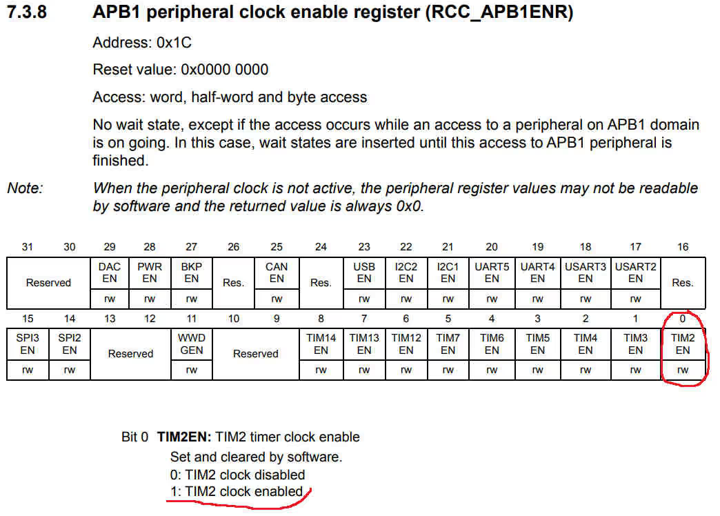
RCC->APB1ENR |= (1<<0); // enable clock for TIM2So all we need to do is write a 1 in the 0th position of the RCC_APB1ENR Register
Now let’s see how to set the presclalar and Auto Reload Register
2. Set Prescalar and ARR
Timers are connected to the Peripheral Clocks. In F103C8, there are 2 peripheral clocks i.e APB1 and APB2. In this tutorial I have decided to use the Timer 2, which is basically connected to the APB2.
We know by now that our system clock is at 72 MHz, and the rest of the clock setup will be as shown below
As shown above, the APB1 Clock is at 72 MHz. The Prescalar is used to bring this clock down to our working range. Here in this tutorial we will be focusing on creating delays in micro and milliseconds, so our working range is around 1 MHz.
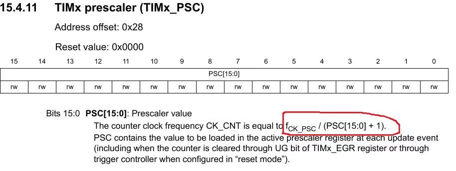
As according to the above formula, If we use the prescalar of 71, the timer clock will come down to [72MHz/(71+1)] = 1 MHz
TIM2->PSC = 72-1; // Prescalar valueAfter setting the timer for 1 MHz, if we start the timer, the counter starts counting from 0.
Each count by the counter takes 1 microsecond. The maximum count this counter can achieve is the value of the ARR.
After this the timer will overflow and our time delay will be messed up.
To avoid this we will keep the ARR value to the maximum possible. This is a 16 bit register, so the maximum value can be 0xffff.
TIM2->ARR = 0xffff-1; // ARR value3. ENABLE the TIMER and wait for CONFIRMATION
In order to enable the Timer, we will modify the Control Register 1 (TIM_CR1).
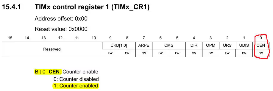
As shown above, the 0th bit of the TIMx_CR1 Register enable the timer, and to do so we need to write a 1 in the 0th position
TIM2->CR1 |= (1<<0); // enable timerTo confirm if the timer has started, we will check the status Register (TIMx_SR)
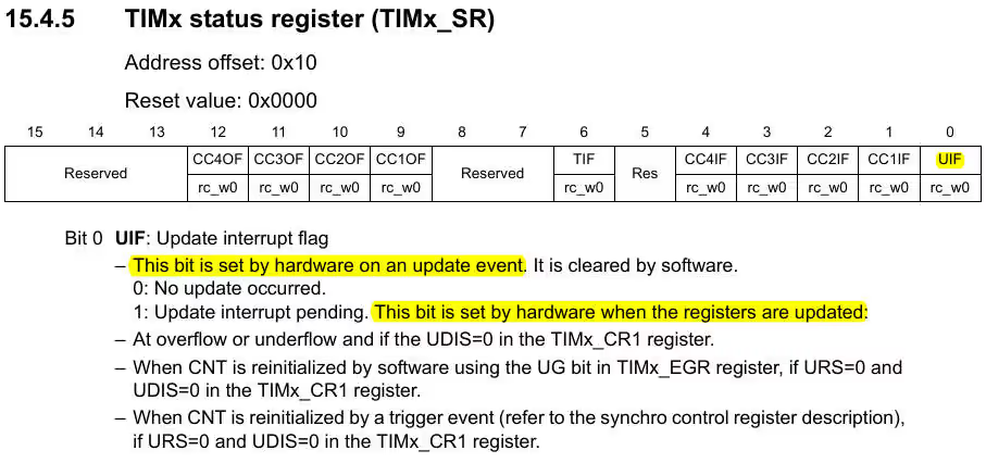
UIF Bit is set whenever there is update event. So we will wait until this bit is set
while (!(TIM2->SR & (1<<0))); // UIF: Update interrupt flag.. This bit is set by hardware when the registers are updatedThis is it for the Timer setup. Let’s configure the GPIO now
GPIO CONFIGURATION
I am using timer 2 to blink a LED, which is connected to PC13. In order to set PC13 as output, we need to follow some set of steps and they are as follows
/************** STEPS TO FOLLOW *****************
	1. Enable the GPIOC clock
	2. Configure the Pin as output
************************************************/1. Enable the GPIOC Clock
To enable the GPIOC clock, we need to modify the APB2 Enable Register (RCC_APB2ENR)
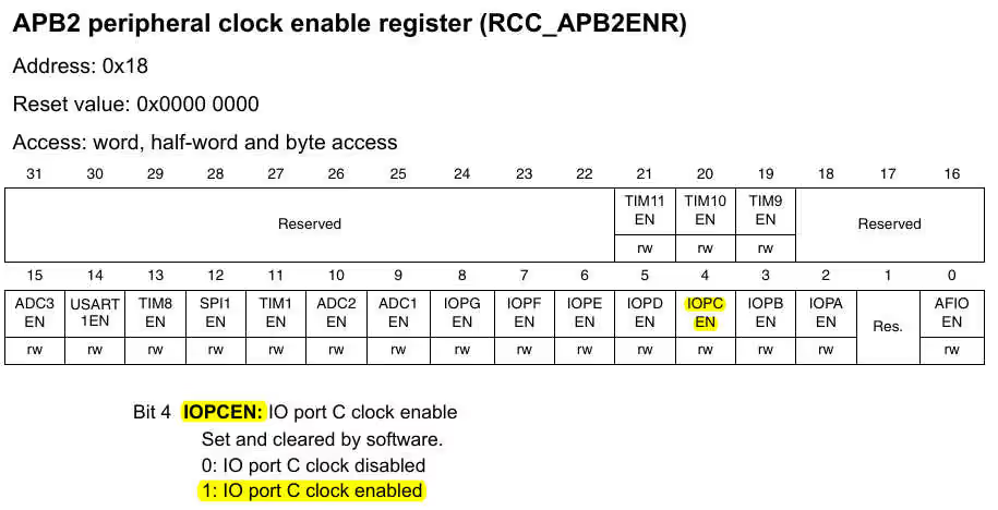
As you can see in the picture above, the 4th bit of RCC_APB2ENR controls the GPIOC Clock. SO we need to write a 1 to the 4th position in order to enable the PORT C clock
RCC->APB2ENR |= (1<<4); // Enable GPIOC Clock2. CONFIGURE the PIN
Now we will configure the pin as output pin. To do this, we need to modify the Port Configuration Register.
This Register is actually divided into 2 categories. Since we are using Pin PC13, we will be using Port configuration register high (GPIOx_CRH). For Pin 0 to 7, we will use GPIOx_CRL
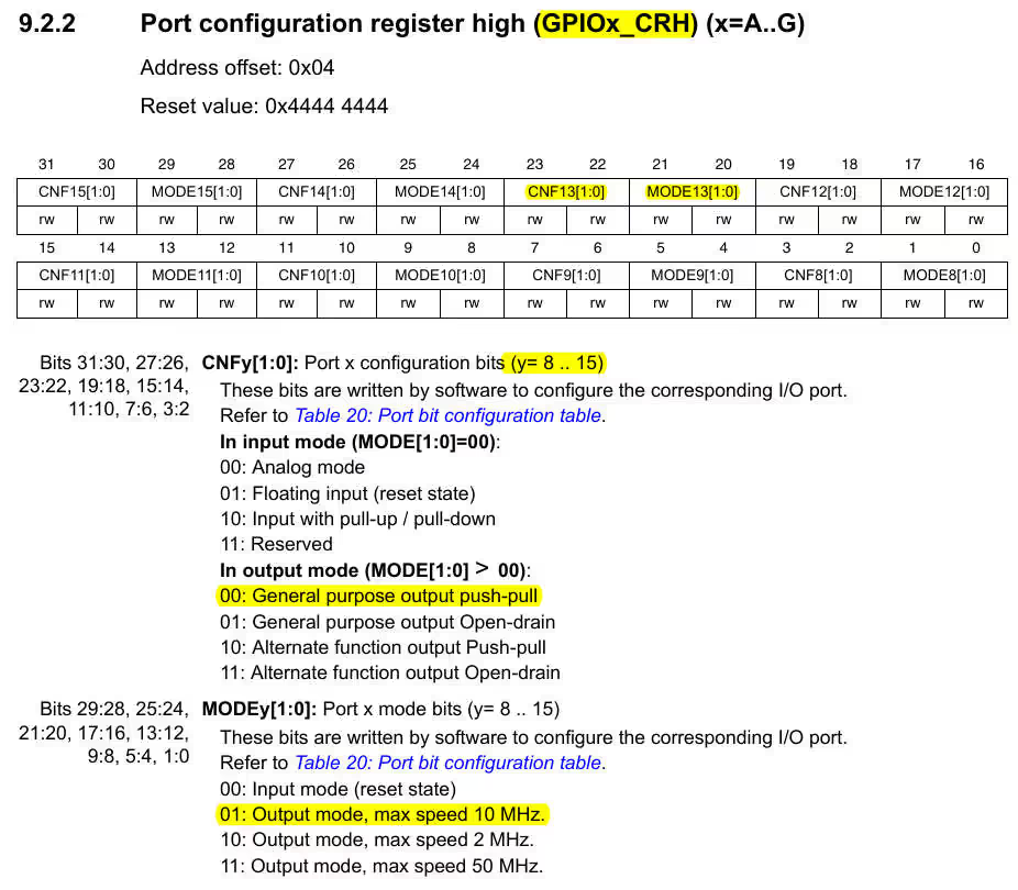
Port Configuration Register controls both, mode and configuration for the Pin. 4 Bits are used to setup a single pin, for example, in order to set up PIN 10, we have to use bits 11:10:9:8
Since we are using the Pin PC13 for blinking the LED, we need to set it as the output mode. I am using the 10 MHz speed for the pin (there is no particular reason for it).
For the configuration part, i am choosing output Push Pull mode, as it’s best to use in simple GPIO operations.
This setup will lead us to configure the bits (23:22:21:20) as 0:0:0:1
GPIOC->CRH &= ~(0xF<<20)  // Clear Bits 23:22:21:20
GPIOC->CRH |= (1<<20); // PC13 Output mode 10 MHz, push pullThe MAIN CODE
int main ()
{
	SystemInit ();
	GPIO_Config ();
	TIM2_Config ();
	while (1)
	{
		GPIOC->BSRR |= (1<<13);  // Set the pin PC13
		Delay_ms (1000);
		GPIOC->BSRR |= (1<<29);  // RESET the pin PC13
		Delay_ms (1000);
	}
}- Here we will first call the SystemInit to configure the clocks
- next GPIO_Config to configure the PC13 as output
- Then TIM2_Config will configure the timer for the delay purpose
Now inside the while loop, we will turn the LED ON and OFF. To handle this, we need to look into the Port Bit Set Reset Register (GPIOx_BSRR)
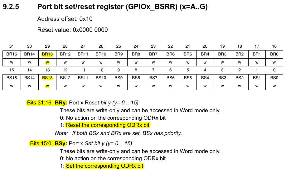
GPIOx_BSRR is a 32 bit Register. The lower 16 Bits (0 to 15) are used to SET the Corresponding Bit. And the upper 16 bits (15 to 31) are used to RESET the corresponding bit
Since we are using PC13, in order to SET this pin, we will write a 1 to the 13th position, and in order to RESET it, we will write a 1 to the 29th position
There is s delay of 1 second between these two statements, and this will keep LED blinking every 1 second
Result
STM32 Register based Tutorial Series

STM32 GPIO Output Example Using Registers | BSRR, MODER, GPIOA Explained

STM32 GPIO Input Configuration – Pin Setup, Pull-Up, and IDR Read
STM32 I2C Tutorial | Register-Based Configuration with Example Code
External Interrupt using Registers

STM32 SPI Tutorial Using Registers (Full-Duplex Master with ADXL345)

DMA with ADC using Registers in STM32

How to Setup UART using Registers in STM32


Hi,
I am new beginner stm32F103c8t6 and i want to use RTC.
How can i set up Low Speed Enable Configuration by using Register manipulation?
Best Regards
Jasem Jamali
Hi,
I am new beginner stm32F103c8t6 and i want to use RTC.
How can i set up Low Speed Enable Configuration?
Best Regards
Jasem Jamali
Enable the GPIOC Clock. register RCC_APB2ENR not from stm32F103, correct
GPIOC->CRH &= ~(0xF<<20) // Clear Bits 23:22:21:20
Sir ” ; ” is missing @ the end of a line on a web page.
hi! i am using stm32f030k6t6 for clock setup register with rcc internal 48 mhz, what is the step? this is equal?
Hello, After connecting ST-Link to Blue-Pill I am getting an Error of “Not an geniune ST Device! Abort Connection.. Can Someone Please Help.. Thanks..
you have the cloned Bluepill. Google that error, thee are some steps to bypass
Hey, where can I find the steps that are needed to set up the clock? Is it available in the reference manual? Thanks.
I wrote them myself
HI ! Loved your tutorials.
I want to ask one thing. Can we use this style of coding(through registers directly) in stm32cube ide also?
I want to use this but I use linux and dont have the option to install keil mkd on linux system.
yes you can, but you have to generate the code through cubeMX (the integrated one). You can delete the content of the main file, and later write the registers only
Hi ! I installed keil 4.7mdk through wine on lubuntu. Tried this code and commented out the delay completely.
Saw the output on oscilloscope, It says the frequency is 2.4Mhz. I expected it to be 36MHz because of the 72Mhz clock of the system. And also the waveform looks like a slowly rising saw tooth wave(this is what surprised me the most though). I wanted to attach waveforms with this comment but no option here.
Then I installed Cube ide. Initialized using MX tool. Using HAL GPIO_Write to toggle pin, checked on scope, freq – 758KHz(square wave).
Then replaced HAL GPIO Write with your code in while loop without delay. This time the freq came out to be 1.6Mhz. But its a nice square wave again.
Can you please explain whats the matter here?
Shouldn’t the output be 32MHz if we assume that controller takes one clock per instruction.
Also is there something that needs to be changed in the initialization part of your code to make it a square wave, because not just at high freq, but also at lower frequencies with your code, the waveform rises slowly for some reason, the falling edge is pretty squared though.
i don’t know about the keil run through wine…
Coming to cubeIDE, like you said you tried the HAL version first. I am sure that the clock setup is wrong in your case. I need more details to solve the issue… you can contact on discord or telegram
Sure. I’ll catch up on discord. Where can I get a link to your discord
Edit: Just saw icon on top right of the page. Thanks
Also tested by replacing the main file in cube ide with your code, had to change the include stm32f1x.h to xx.h in both delay and main.
the output wave is 307KHz now. And the problem of slowly rising edge persists even at this frequency.
This low frequency makes me think that the clock might be set to 8MHz instead of 72MHz for some reason. This is my first day trying stm so don’t know how to do stuff here.
Have you tried using plain register access in cube ide. What changes might be needed here
Lastly replaced the whole code in main file in cube ide with your code, removed all the hal related files, only CMSIS folder remains inside Drivers.Had to add stm32f10x.c and .h and a couple of files from the keil installation folder to stm32cube project to make it compile.
The code compiled and the output is again a slowly rising(falling edge is square though) saw tooth wave. commented out the delay lines, the ffrequency came out to be 1.85MHz.
So my last question would be, why are the results so different for the exact same code compiled from keil and cubeide.
Keil- 2.4MhZ Saw Tooth Wave
Cubeide-
MX and HAL – 758KHz Square Wave
HAL initialization but direct register access inside while- 1.6MHz Square Wave
Removed HAL and replaced whole code with keil code -1.85MHz Saw Tooth
The link to telegram and discord are on the top right of the website
If you are planning to exclusively use CMSIS, try embedded studio. I find it stable on Ubuntu, a good alternative to Keil. Some things will be different.
You will need a bit of a set-up to use ST-Link as a debugger, but you can flash J-Link on a disco board.
GPIOC->CRH |= (1<<20); // PC13 output open drain mode
GPIOC->CRH = 0x44344444; // PC13 general purpose output push-pull
Thanks.. Updated
How did you find the push pull hex. Can you please help?