
Home ▸ STM32 Tutorials ▸
Updated On: September 14, 2025
STM32 Clock Configuration with Registers – RCC Setup Example
This tutorial explains how to perform STM32 clock configuration using registers only, without HAL, SPL, or LL libraries. Many developers search for stm32 clock configuration, rcc register setup, and stm32 maximum system clock examples, so we’ll cover them step by step. We’ll configure the RCC registers, enable HSE, set PLL parameters, prescalers, and flash latency to achieve the maximum clock speed (180 MHz for STM32F4). By the end of this guide, you’ll understand how to manually program the STM32 RCC configuration to bring up the system clock from scratch.
Welcome to this new STM32 Register tutorial series, where we will program the STM32 microcontroller directly by working with its Registers, without using any libraries such as HAL, SPL, or LL.
This is the first and one of the most important tutorials in the series. Today, we will focus on learning how to configure and set up the clock.
R307 Fingerprint Module Video Tutorial
While the written guide below provides all the details and code for reference, sometimes a visual demonstration can make all the difference. I’ve created a complete video walkthrough that runs through the entire process in real-time. Follow the written steps here while watching the implementation in the video to solidify your understanding and catch any subtle details
Watch the VideoParts and software Required
I am going to use Keil IDE for the STM32 Register programming. It is a paid IDE but it offers a free version (MDK-Lite), which is limited to 32 KB of code size. This is enough for our register based programming.
I am also using STM32F4 series MCU for these projects but I will also explain the process for STM32F1 series MCUs. You can find the required parts at the links below.
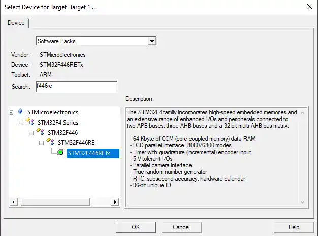
Create the Project in Keil IDE
Let’s begin by creating a project in Keil and selecting the appropriate microcontroller.
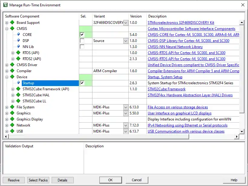
Next, we need to include some essential files in the project. Select the CMSIS core and the Device Startup files, as shown below.
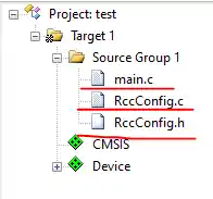
Then, add the main file to the project. Along with it, I have also included RccConfig.h and RccConfig.c. These files will contain the code for the clock setup and can be reused directly in our future projects.
Step-by-Step STM32 RCC Configuration (Register Level)
Since setting up the clock can be a complex process, for today’s tutorial we will use some information from CubeMX. Follow along carefully:
- Open CubeMX.
- Select your STM32 microcontroller.
- Under RCC settings, choose the external crystal.
- Set the HCLK to its maximum value and confirm your selection.
- Keep CubeMX open, as we will refer to it shortly.
- Next, create a new project in Keil and select the same microcontroller.
Below are the step-by-step instructions for setting up the clock:
	/*************>>>>>>> STEPS FOLLOWED <<<<<<<<************

	1. ENABLE HSE and wait for the HSE to become Ready
	2. Set the POWER ENABLE CLOCK and VOLTAGE REGULATOR
	3. Configure the FLASH PREFETCH and the LATENCY Related Settings
	4. Configure the PRESCALARS HCLK, PCLK1, PCLK2
	5. Configure the MAIN PLL
	6. Enable the PLL and wait for it to become ready
	7. Select the Clock Source and wait for it to be set

********************************************************/Let’s go through each step one by one.
1. Enable HSE and wait for the HSE to become Ready
The HSE can be configured in the RCC_CR Register as you can see below

As you can see the 16th bit of this register can enable the HSE, and the 17th bit will set to 1, when the HSE is finally ready
RCC->CR |= 1<<16;
while (!(RCC->CR & (1<<17)));above, I have set the bit 16 to HIGH (to enable the HSE), and then I am waiting for the 17th bit to set HIGH (HSE to become Ready)
2. Set the POWER ENABLE CLOCK and VOLTAGE REGULATOR
The Power Enable Clock can be set in the RCC_APB1ENR Register as shown in the picture below
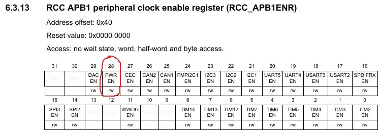
In order to enable the Power, i need to set the bit 28 of the RCC_APB1ENR Register
RCC->APB1ENR |= 1<<28;The Voltage Regulator can be configured in the PWR_CR Register as shown below
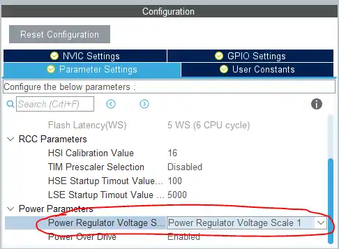
In the RCC setup of the CubeMX, the voltage Regulator is selected for scale 1 by default. And i will also use the same for my application. Basically I need to write a 3 (11) in the 14th bit
PWR->CR |= 3<<14; 3. Configure the FLASH PREFETCH and the LATENCY Related Settings
The settings are as shown in the RCC setup from the CubeMX below
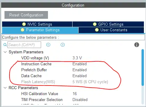
To configure them, we need to look in the FLASH_ACR Register
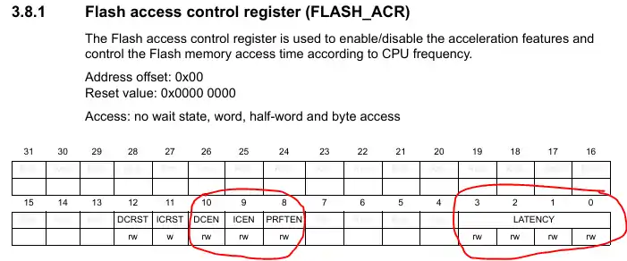
As shown in the CubeMX picture above, the Instruction Cache, Prefetch Buffer, and the Data Cache all are enabled. Also the Flash Latency is 5WS
So i need to write a 1 in the 8th, 9th and the 10th positions. Also a 5 in the 0th position (for 5WS)
FLASH->ACR = (1<<8) | (1<<9)| (1<<10)| (5<<0);4. Configure the PRESCALARS HCLK, PCLK1, PCLK2
Here we will set the values for AHB Prescalar, APB1 Presclar, and APB2 Prescalar
The values are shown below (in RED color) in the Clock Setup from the CubeMX
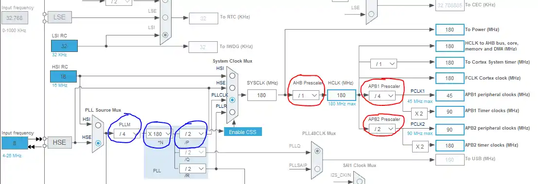
To configure them, we will look into the RCC_CFGR Register

As shown in the CubeMX setup above
- The AHB Prescalar is 1, so the HPRE (bits 7:4) will be all 0s.
- APB1 Prescalar is 4, so the PPRE1 (bits 12:10) will be “101” i.e write 5 to the 10th position
- APB2 Prescalar is 2, so the PPRE2 (bits 15:13) will be “100” i.e write 4 to the 13th position
// AHB PR
RCC->CFGR &= ~(1<<4);
// APB1 PR
RCC->CFGR |= (5<<10);
// APB2 PR
RCC->CFGR |= (4<<13);5. Configure the MAIN PLL
Here we will configure the PLL source (HSE or HSI), and also set the values for PLLM, PLLN and PLLP
The vales are shown below (in the BLUE color)
The configuration can be set in the RCC_PLLCFGR Register
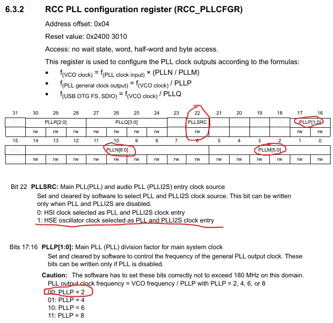
We can directly push the required values to the PLLM and PLLN Bits, while the care must be taken when setting the PLLP value.
- The PLLP value, according to the CubeMX is 2, and to set it, I need to write 0s in the PLLP (Bits 17:16)
- PLLM and PLLN values are 4 and 180, according to the CubeMX, and I will directly set them in the PLLM (Bits 5:0) and PLLN (Bits 14:6)
- As I am using HSE crystal for the clock, I need to set the PLLSRC (Bit 22) to 1.
#define PLL_M 4
#define PLL_N 180
#define PLL_P 0 // PLLP = 2
RCC->PLLCFGR = (PLL_M <<0) | (PLL_N << 6) | (PLL_P <<16) | (1<<22);6. Enable the PLL and wait for it to become ready
The PLL can be enabled in the RCC_CR Register as shown below
To enable the PLL, we must write a 1 to the PLL ON (24th bit), and then we will wait for the PLL RDY (25th bit) to set, which will indicate that the PLL is ready.
RCC->CR |= (1<<24);
while (!(RCC->CR & (1<<25)));7. Select the Clock Source and wait for it to be set
The clock source can be selected in the RCC_CFGR Register
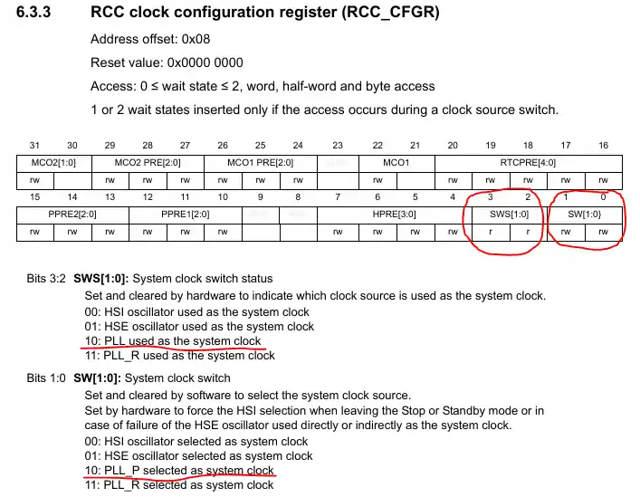
- SW[1:0] is used to set the system clock. Since I am using the PLL_P as the system clock, I will write a 2 (1:0) to the SW Bits
- SWS[3:2] is used to monitor the status of the system clock. So here we will wait for these bits to indicate that the PLL_P has been set as the system clock (wait for the SWS bits to indicate 2 (1:0)).
RCC->CFGR |= (2<<0);
while (!(RCC->CFGR & (2<<2)));That completes the setup process. The above setup will allow my controller to run at 180 MHz, as I did setup in the cubeMX
The main Function
We will test the clock configuration by blinking a LED. I am using Nucleo F401 and the LED on this board is connected to pin PA5. Below is the implementation of the main function.
int main (void)
{
SysClockConfig ();
GPIO_Config ();
while (1)
{
GPIOA->BSRR |= (1<<5); // Set the pin PA5
delay (20000000); // some random Delay
GPIOA->BSRR |= ((1<<5) <<16); // Reset pin PA5
delay (20000000);
}
}The program starts with the main function. Inside it, the system clock is configured by calling SysClockConfig(), and the GPIO pins are set up by calling GPIO_Config(). This ensures the microcontroller is running at the desired speed and the required pin is ready for use.
We have already covered the system clock configuration in this tutorial and the GPIO configuration will be covered in the next one.
After the setup, the program enters an infinite while(1) loop. This loop runs continuously as long as the microcontroller is powered.
Inside the loop:
GPIOA->BSRR |= (1<<5);sets pin PA5 to a HIGH state, which turns the connected LED ON.- A delay is added so that the LED stays visible in the ON state for some time.
GPIOA->BSRR |= ((1<<5)<<16);resets pin PA5 back to LOW, which turns the LED OFF.- Another delay is added so the LED remains OFF for a while.
By repeating this process, the LED connected to PA5 will blink continuously, controlled entirely by register-level programming.
Common STM32 Clock Configuration Issues
Developers often face problems during manual RCC setup:
- Wrong PLL values → CPU won’t reach target frequency.
- Flash latency misconfigured → MCU hangs or resets.
- Not waiting for HSE/PLL ready flags → unstable system clock.
- Overclocking STM32 beyond datasheet → unexpected crashes.
Always cross-check with CubeMX clock tree and STM32 reference manual.
Result
The gif below shows the output of the above code.

As you can see, the LED on the board is blinking, which confirms that the clock has been successfully configured. However, we still need to verify whether the clock is running at the exact frequency we set. We will check this in another tutorial, where we will configure a Timer to generate precise delays in both microseconds and milliseconds.
With this setup, you now know how to configure the STM32 system clock using registers. We enabled the HSE, set up the PLL, configured prescalers and flash latency, and finally selected the PLL as the system clock. This configuration runs the STM32F4 at 180 MHz, the maximum frequency supported. Direct RCC register programming not only improves your understanding of microcontroller clocking but also gives you full control without relying on CubeMX or HAL. In upcoming tutorials, we’ll extend this to topics like clock security system (CSS) and low-power clock configurations for STM32.
STM32 Register based Tutorial Series
STM32 GPIO Output Example Using Registers | BSRR, MODER, GPIOA Explained

STM32 GPIO Input Configuration – Pin Setup, Pull-Up, and IDR Read
STM32 I2C Tutorial | Register-Based Configuration with Example Code
External Interrupt using Registers

STM32 SPI Tutorial Using Registers (Full-Duplex Master with ADXL345)

DMA with ADC using Registers in STM32

How to Setup UART using Registers in STM32
PROJECT DOWNLOAD
Project FAQs


In your development board, the crystal is not connected in X3 and c33, c34 capacitors are not connected. I don’t understand how you used it as an external crystal.
void SwitchToHSI_1MHz(void) {
// // Enable HSI
// __HAL_RCC_HSI_ENABLE();
// printf(“HSI is Enabled \r\n”);
// // Wait for HSI to be ready
// while (__HAL_RCC_GET_FLAG(RCC_FLAG_HSIRDY) == RESET);
// printf(“HSI is READY. Proceeding with switch…\r\n”);
// Disable PLL (if enabled)
__HAL_RCC_PLL_DISABLE();
printf(“PLL is Disabled\r\n”);
// Configure HSI to run at 1 MHz (Divide by 16)
RCC_OscInitTypeDef RCC_OscInitStruct = {0};
RCC_OscInitStruct.OscillatorType = RCC_OSCILLATORTYPE_HSI;
RCC_OscInitStruct.HSIState = RCC_HSI_ON;
RCC_OscInitStruct.HSICalibrationValue = RCC_HSICALIBRATION_DEFAULT;
RCC_OscInitStruct.HSIDiv = RCC_HSI_DIV16; // Divide by 16 to get 1 MHz
RCC_OscInitStruct.PLL.PLLState = RCC_PLL_NONE;
printf(“Enabling HSI…\r\n”);
__HAL_RCC_HSI_ENABLE();
while (__HAL_RCC_GET_FLAG(RCC_FLAG_HSIRDY) == RESET); // Wait until HSI is ready
printf(“HSI is now enabled.\r\n”);
// Apply oscillator configuration
if (HAL_RCC_OscConfig(&RCC_OscInitStruct) != HAL_OK) {
printf(“Oscillator configuration failed!\r\n”);
} else {
printf(“Oscillator configuration successful!\r\n”);
not working from here /////////////////////////////////////////////////////////////////
HAL_Delay(30);
// Switch System Clock to HSI (1 MHz)
RCC_ClkInitTypeDef RCC_ClkInitStruct = {0}; // Initialize structure to zero
RCC_ClkInitStruct.ClockType = RCC_CLOCKTYPE_HCLK | RCC_CLOCKTYPE_SYSCLK | RCC_CLOCKTYPE_PCLK1;
RCC_ClkInitStruct.SYSCLKSource = RCC_SYSCLKSOURCE_HSI; // Set SYSCLK to HSI
RCC_ClkInitStruct.AHBCLKDivider = RCC_SYSCLK_DIV16; // Divide HSI (16 MHz) by 16 → 1 MHz
RCC_ClkInitStruct.APB1CLKDivider = RCC_HCLK_DIV1; // Keep APB1 clock unchanged
// Apply Clock Configuration
HAL_StatusTypeDef status = HAL_RCC_ClockConfig(&RCC_ClkInitStruct, FLASH_LATENCY_1);
if (status != HAL_OK) {
printf(“Clock configuration failed! Error Code: %d\r\n”, status); // Include error code
} else {
printf(“Clock configuration Successful\r\n”);
}
}
At step 5. Configure the MAIN PLL ive noticed that you do not set RCC-PLLCFGR bit 22 to 1 so that the PLL is fed from HSE. Is there a reason for that or could it be that I am wrong or missed something ? THANKYOU.
Never mind. It was there but i didnt see it. Thanks !
Hi, I downloaded code and flash my Nucleo-F446RE board. The LED remains ON all the time, no blinking.
Further, I also commented in the program:- Pin OUTPUT and while loop (shown below). still the LED is ON. I am surprised. What could be the reason, if any one have encountered this ? thank you
// 2. Set the Pin as OUTPUT
//GPIOA->MODER |= (1<BSRR |= (1<BSRR |= ((1<<5) <<16); // Reset pin PA5
delay (20000000);
} */
Hi Sir , i did already ask my question on the Youtube .. Im really stuck , when i wrote these codes – my card is STM32F4 Discovery Board , My CPU is STM32F407VET6- my PLL values doesnt changed
.
void my_clock_config()
{
	/*************>>>>>>> STEPS FOLLOWED <<<<<<<<************

	1. ENABLE HSE and wait for the HSE to become Ready
	2. Set the POWER ENABLE CLOCK and VOLTAGE REGULATOR
	3. Configure the FLASH PREFETCH and the LATENCY Related Settings
	4. Configure the PRESCALARS HCLK, PCLK1, PCLK2
	5. Configure the MAIN PLL
	6. Enable the PLL and wait for it to become ready
	7. Select the Clock Source and wait for it to be set

	********************************************************/
//1.Enable HSE and wait for the HSE become Ready
RCC->CR |= 1<<16;
while(!(RCC->CR & (1<<17)));
//2.Set the POWER ENABLE CLOCK and VOLTAGE REGULATOR
RCC->APB1ENR |= 1<<28; //Power Enabled – internal powe-
PWR->CR |= 1<<14; //VOS :1 = Scale 1 mode as is default
//3.Configure the FLASH PREFETCH and the LATENCY Related Settings
FLASH->ACR |= 1<<8;
FLASH->ACR |= 1<<9;
FLASH->ACR |= 1<<10;
FLASH->ACR |= 5<<0;
//4.Configure the PRESCALARS HCLK, PCLK1, PCLK2
RCC->CFGR &= ~(1<<4);
RCC->CFGR |= 5<<10;
RCC->CFGR |= 4<<13;
//5. Configure the MAIN PLL
RCC->PLLCFGR |= 4<<0;
RCC->PLLCFGR |= 168<<6;
RCC->PLLCFGR |= 0<<16;
RCC->PLLCFGR |= 1<<22; //Choosing HSE for PLL source
//6. Enable the PLL and wait for it to become ready
RCC->CR |= 1<<24;
while(!(RCC->CR & (1<<25)));
//7. Select the Clock Source and wait for it to be set
RCC->CFGR |= 2<<0;
while(!(RCC->CFGR & (2<<2)));
}
Are you confused with the HSE for the PLL source?
I mean it should be PLL source: RCC->PLLCFGR |= 2<<22.
I’m getting quite distracted and swamped by all the ads here. Is it possible to download this tutorial presentation ?
There is a download button(above the comment section) to download the code.
If you want to read the whole article, then press cntrl+s to save the webpage, which you can read later.
I know the ads are distracting and I am working on it. There is some testing going on and it will remain for another 20 days. After that the site will be stable (in terms of ads).
please tell me how could I know that the clock needs to be set in this order, if there was no this article? Where are these steps in the manual? Or how to use it to understand that everything needs to be done in that order? And
These steps are not mentioned anywhere, neither you could find them easily on the internet. If you want to learn these things, you have to start from the basic ARM devices like arm V6 / V7. Then move to 32 bit arm controllers and finally to STM32..
I have STM32F103C6T6A but couldn’t find the header file for this module. Should I get the exact stm32f446? or i can do it with this one?
check out the tutorial for F103. It might be the closest available
https://controllerstech.com/stm32f103-clock-setup-using-registers/
Thank you very much, this tutorial helped me a lot … is it possible somehow to verify the modified clock speed ? e.g. in the debug mode (I use STMcubeIDE
Thank you again
Yes, you can do that through MCO1 If you kneed info on how to then let me know.
thank you very much. It was very helpful.
Thank you for awesome lessons, sir. i will continue to learn from you.
Dear Sir,
Where do you set HSE Frequency ? I couldn’t find it in this code
I guess I have answered it on youtube..
these two lines ensures the proper power delivery to the MCU relating to the oscillator circuit, basically the external oscillator, which is fixed value by board design, the board he used has a 8mhz oscillator shared between st link and main mcu, that’s why he typed 8mhz in cubemx clock configuration flow chart. if u design a board with 16 mhz external oscillator then the HSE input clock would be 16mhz instead of 8mhz and to achieve max frequency u need to change PLL M,N,P etc and other Prescaler values to delivar the clock in different buses that avails clock for different peripherals.
i’m using f429 discovery board by weave share electronics and it has separate ocillator for st link and main MCU HSE input, both are 8mhz.
so this is external hardware, u can’t define the input as much u wish .
Dear Sir,
How to find Step by Step for each peripheral?
Thanks!
Dear Sir,
RCCclock_config.c & RccClock_config.h are not included in the download file. Is it neccessary to have it in order to run the code?
those files were not mentioned in this tutorial. Actually I created those files after writing this one.
There is a sysclockconfig function in the main file, which takes care of the RCC configuration
I created rccconfig.c in the second tutorial (you can check the second video in the playlist) so that it would be easier to include them in upcoming tutorials
Hello, I have STM32F4 Discovery but I have difficulties setting up the clock. I checked the reference manuals for register differences, I checked the syntax but I didn’t find any problems. When I download the code to the Discovery Board regardless of the delay function my LEDs (I tried the ones on the board and 3.5mm ones.) just lights up dim and doesn’t blink or do anything really. Can you help with this ?
The LED might be staying ON because the delay between the blink is low. You should debug your code and then check if the LED is turning OFF or not
Dear Sir,
4. Configure the PRESCALARS HCLK, PCLK1, PCLK2
The AHB Prescalar is 1, so the HPRE (bits 7:4) will be all 0s.
So in that case, i think
RCC->CFGR &= ~(F<<4);
But you mentioned
So why you only makes 4 bit zero.
Please explain.
My bad. It should have been ~(F<<4). Since the default values in those bits is anyway 0, i didn’t bother too much, as i just wanted to show that we need to write 0’s there..
Thanks for your explanation.