Home ▸ STM32 Tutorials ▸
Updated On: March 23, 2026
How to Erase Sectors
This is the 3rd tutorial in the W25Q Flash series, and today we will see how Erase sectors. In the previous tutorial we read the data stored in the sector 0 and sector 1. Today we will erase those sectors and read the data again. This way we will confirm if the data has been erased or not.
Erasing a sector is important before we learn about writing data into the flash memory. According to the datasheet of the module, we can only write the data at some location, if it has been erased (current data is 0xFF). Also a sector is the smallest memory that we can erase.
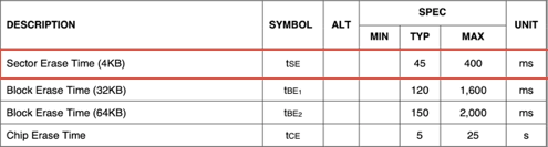
That means we can not erase a particular memory byte, or even a page. Although we can erase a complete sector (16 pages), or a 32 KB memory block (8 sectors), or a 64 KB memory block (16 sectors), or even a complete chip. But the higher the memory block we erase, the more time consuming the process is.
For getting started, erasing a sector is good enough and it only takes 400ms to do so. This information is provided in the datasheet of the device.
Although the connection has already been explained in the previous tutorials, let’s see it again here.
VIDEO TUTORIAL
You can check the video to see the complete explanation and working of this project.
Connection
The W25Q NOR Flash memories can use the SPI in Single/Dual/Quad mode. For the simplicity of the operation, we will stick to the Single SPI mode, where we would need 4 pins to connect the Flash with the controller.
The connection diagram between the Flash module and the STM32 is shown below.
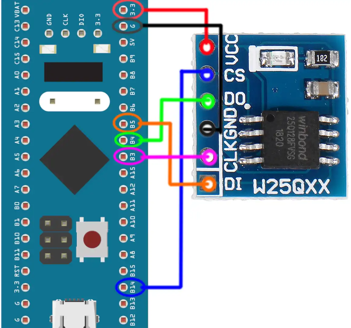
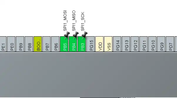
- The CS (Chip Select) Pin is connected to the pin PB14. It will be used to select or unselect the slave Device.
- The DO (Data Out) pin is connected to the pin PB4 (MISO). The device outputs the data on this pin
- The CLK (Clock) pin is connected to the pin PB3 (CLK). The clock is used to synchronise the master and the slave device.
- The DI (Data In) pin is connected to the pin PB5 (MOSI). The master send the data to the device on this pin.
- The Device is powered with 3.3v from the MCU itself.
The Module provides 6 pins (including the Vcc and Gnd). But the chip has 8 pins in total. If you have the chip rather than the module, you can connect it as shown below.
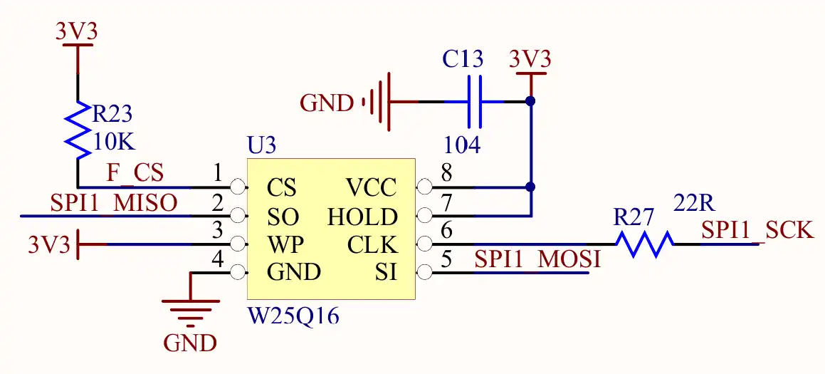
Note that the WP (Write Protect) pin is active Low pin, so it must be pulled HIGH when you want to modify the flash, and pulled LOW when you want to disable the modification.
The connections shown above are for the Single SPI mode, not for Dual or Quad modes.
CubeMX Setup
We will enable the SPI in Full Duplex master mode. The configuration is shown below.
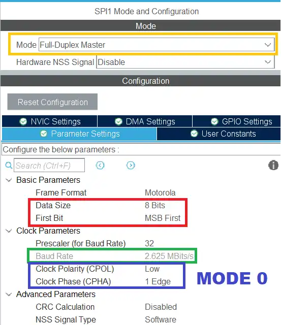
The Data width is set to 8 bits and the data should be transferred as the MSB first. The prescaler is set such that the Baud Rate is around 2.5 Mbits/sec.
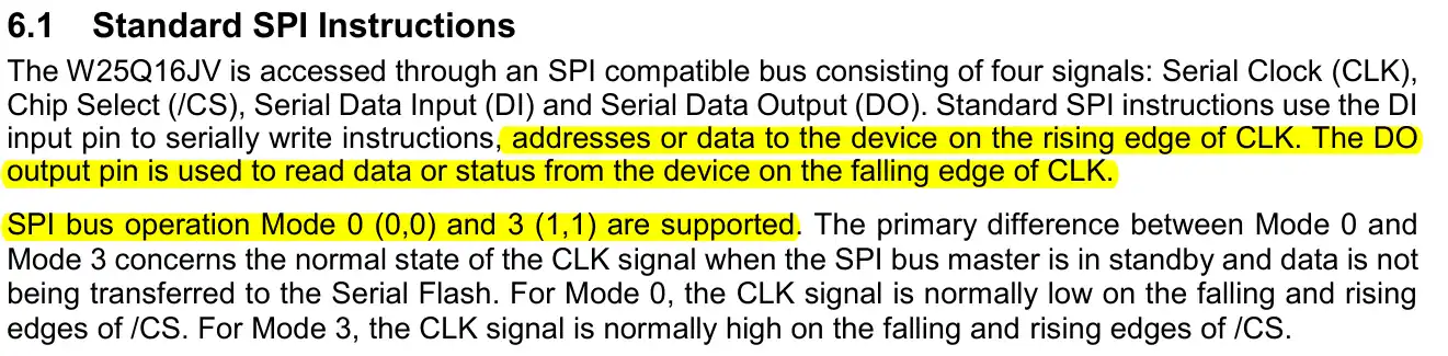
According to the datasheet of the W25Q Flash, the SPI Mode 0 and Mode 3 are supported. Below is the image from the datasheet.
In the SPI configuration, we keep the Clock Polarity (CPOL) low and the Clock Phase (CPHA) to 1 edge. Here 1 edge means that the data will be sampled on the first edge of the clock. And when the CPOL is Low, the first edge is the rising edge. Basically we are using the SPI Mode 0.
In Full duplex Mode, SPI uses 3 pins, MOSI, MISO and CLK. We need to set one more pin as output so to be used as the Chip Select (CS) Pin.
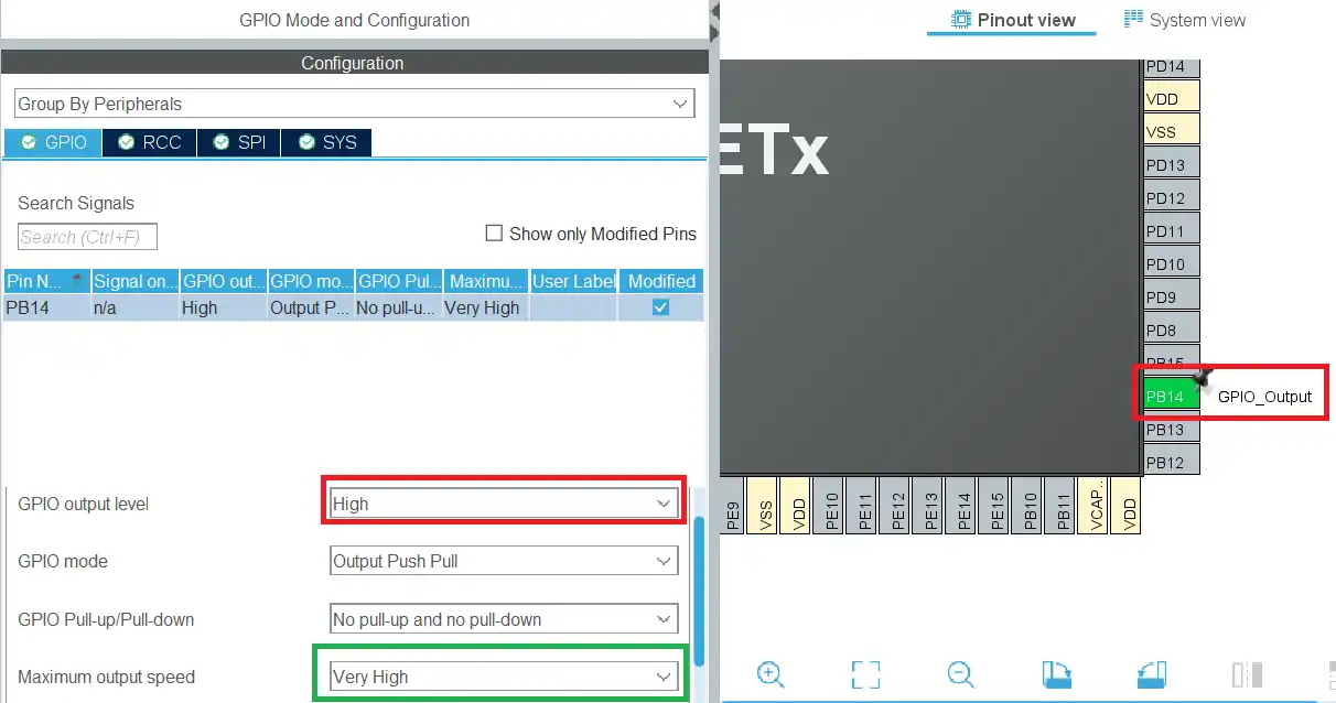
The Pin PB14 is set as the CS pin. The initial output level is set to HIGH. This is because the pin needs to be pulled low in order to select the slave device, so we keep it high initially to make sure the slave device isn’t selected. The Output speed is set to Very High because we might need to select and unselect the slave at higher rate.
We created separate library files for the device. Today we will simply update the code in these files itself.
The files are: W25Qxx.c file in the src directory and W25Qxx.h file in the Inc directory.
Let’s Write the Code
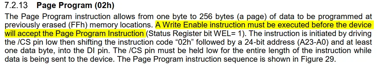
According to the datasheet before executing the Page program command, we must execute the write enable instruction. This is shown in the image below
Write Enable
The write enable instruction must be executed prior to every Page Program, Sector Erase, Block Erase, Chip Erase, Write Status Register and Erase/Program Security Registers instruction. The instruction is shown below.
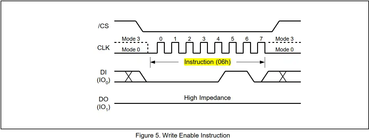
Below is the function to enable the write.
void enable_write (void)
{
	uint8_t tData = 0x06;  // enable Write
	csLOW();  // pull the CS LOW
	SPI_Write(&tData, 1);
	csHIGH();  // pull the HIGH
	W25Q_Delay (5);  // Write cycle delay (5ms)
}We simply send the instruction (0x06) to the device. This enables the write and we can perform the page write or erasing operations after this.
Just like write enable, there is an instruction to disable the write also. Below is the code for the same.
void disable_write (void)
{
	uint8_t tData = 0x04;  // disable Write
	csLOW();  // pull the CS LOW
	SPI_Write(&tData, 1);
	csHIGH();  // pull the HIGH
	W25Q_Delay (5);  // Write cycle delay (5ms)
}The instruction is performed in the similar way as the write enable instruction, except the instruction (0x04) is different. Note that the write is automatically disabled after Power-up and upon completion of the Write Status Register, Erase/Program Security Registers, Page Program, Sector Erase, Block Erase, Chip Erase and Reset instructions. I am just including it so as to perform the safe operations.
Erase Sectors
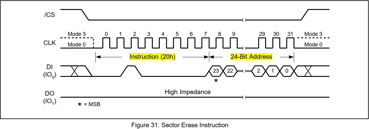
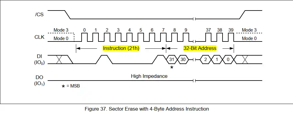
The erase sector instruction (0x20) is sent along with the memory address, whose sector should be erased. We send the instruction (0x21) for the same, but for the 32bit memory addresses (size>=256Mb). The Sector Erase instruction sets all memory within a specified sector (4K-bytes) to the erased state of all 1s (0xFF). A Write Enable instruction must be executed before the device will accept the Sector Erase Instruction.
void W25Q_Erase_Sector (uint16_t numsector)
{
	uint8_t tData[6];
	uint32_t memAddr = numsector*16*256;   // Each sector contains 16 pages * 256 bytes

	write_enable();

	if (numBLOCK<512)   // Chip Size<256Mb
	{
	  tData[0] = 0x20;  // Erase sector
	  tData[1] = (memAddr>>16)&0xFF;  // MSB of the memory Address
	  tData[2] = (memAddr>>8)&0xFF;
	  tData[3] = (memAddr)&0xFF; // LSB of the memory Address

	  csLOW();
	  SPI_Write(tData, 4);
	  csHIGH();
	}
	else  // we use 32bit memory address for chips >= 256Mb
	{
	  tData[0] = 0x21;  // ERASE Sector with 32bit address
	  tData[1] = (memAddr>>24)&0xFF;
	  Data[2] = (memAddr>>16)&0xFF;
	  tData[3] = (memAddr>>8)&0xFF;
	  tData[4] = memAddr&0xFF;

	  csLOW();  // pull the CS LOW
	  SPI_Write(tData, 5);
	  csHIGH();  // pull the HIGH
	}

	W25Q_Delay(450);  // 450ms delay for sector erase

	write_disable();

}The parameter of the function is the number of sector that we want to erase.
- We first calculate the memory address using the sector number. Each sector contains 16 pages and each page contains 256 bytes.
- The memory address could be 24bit / 32bit depending on the memory size of the device.
- We use different commands for both address sets. 0x20 for the 24 bit memory addresses and 0x21 for the devices with 32bit memory addresses.
- Before sending the erase command, we enable the write.
- To erase the sector we send the instruction followed by the memory address.
- The sector erase time is 400ms, so we wait for the erase to complete.
- At last disable the write.
The main function
  W25Q_Read(1, 85, 20, RxData);
  // Read the data from page 1, 85
  W25Q_Erase_Sector(0);
  // erase sector 0
W25Q_Read(1, 85, 20, RxData); // Read the data againWe use the same code from the previous tutorial, where we read the data from 2 different sectors. We erase the sector 0 and sector 1, and again read the data.
If the sectors gets erased, we should receive the data 0xFF instead of what was stored in those positions.
Result
Below the images shows the data received, before and after performing the sector erase.
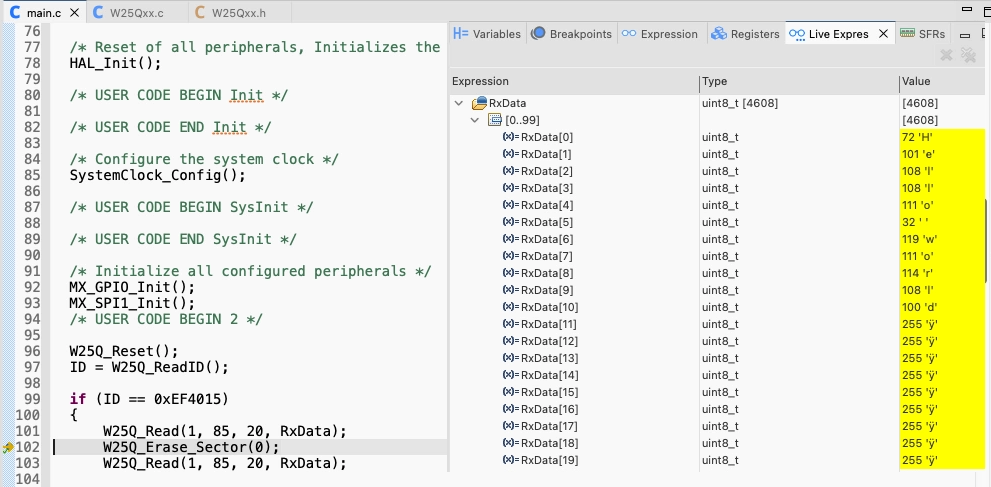
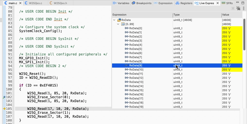
As you can see the data stored on page 1, 85 was “Hello world”. But after erasing the sector 0, the entire data was erased and we received 0xFF (255) from that location.
The video below shows the working in more detail.
STM32 W25Q Flash Tutorials Series

W25Q Flash Series Part 2 – Read Data from Device
W25Q Flash Series Part 4 – How to Program Pages
W25Q Flash Series Part 5 – how to update sectors
W25Q Flash Series Part 6 – Integers floats and 32bit Data
W25Q Flash Series Part 7 – QUADSPI Write, Read, Memory Mapped mode
W25Q Flash Series Part 8 – QUADSPI External Loader
W25Q Flash Series Part 9 – SPI Flash Loader


I am seeing the following code:
if (numBLOCK<512) // Chip Size<256Mb{
}void W25Q_Read (uint32_t startPage, uint8_t offset, uint32_t size, uint8_t *rData)
{
uint8_t tData[5];
uint32_t memAddr = (startPage*256) + offset;
if (numBLOCK<512) // Chip Size<256Mb
{
tData[0] = 0x03; // enable Read
tData[1] = (memAddr>>16)&0xFF; // MSB of the memory Address
tData[2] = (memAddr>>8)&0xFF;
tData[3] = (memAddr)&0xFF; // LSB of the memory Address
}
How 3 byte-address can access 256Mb, i.e 32MB? I think it should be 16MB?
It can not access 256Mb. The code says <256Mb (not including 256Mb), while if you continue reading further, the next instructions are for >=256Mb.
There are no devices between 128Mb and 256Mb, therefore the 3 byte address is valid for upto 128Mb.