Home ▸ STM32 Tutorials ▸
Updated On: March 23, 2026
How to Read data from W25Q Flash Memory
This is the 2nd tutorial in the W25Q Flash series, and today we will see how to perform the read operation to read the data stored in the Flash memory. We will read the data from an offset, where the data is actually stored, and also from the beginning of the memory.
The W25Q Flash memories offers different Read options that include simple Read and Fast Read. The Fast Read is similar to the Read except that it can operate at the highest possible frequency. We will cover both these methods in today’s tutorial.
In the previous tutorial we saw how to make the connection and how to read the device ID. We will continue edit the library files we created in the previous tutorial, the W25Qxx.c and W25Qxx.h files.
Let’s take a look at the connection again.
VIDEO TUTORIAL
You can check the video to see the complete explanation and working of this project.
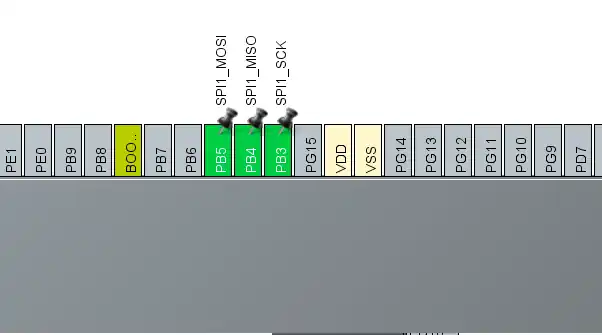
Connection
The W25Q NOR Flash memories can use the SPI in Single/Dual/Quad mode. For the simplicity of the operation, we will stick to the Single SPI mode, where we would need 4 pins to connect the Flash with the controller.
The connection diagram between the Flash module and the STM32 is shown below.
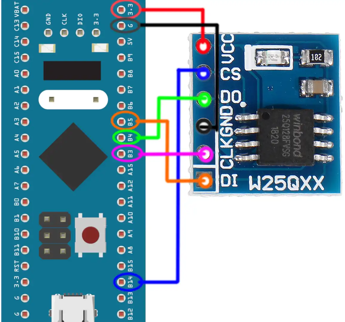
- The CS (Chip Select) Pin is connected to the pin PB14. It will be used to select or unselect the slave Device.
- The DO (Data Out) pin is connected to the pin PB4 (MISO). The device outputs the data on this pin
- The CLK (Clock) pin is connected to the pin PB3 (CLK). The clock is used to synchronise the master and the slave device.
- The DI (Data In) pin is connected to the pin PB5 (MOSI). The master send the data to the device on this pin.
- The Device is powered with 3.3v from the MCU itself.
The Module provides 6 pins (including the Vcc and Gnd). But the chip has 8 pins in total. If you have the chip rather than the module, you can connect it as shown below.
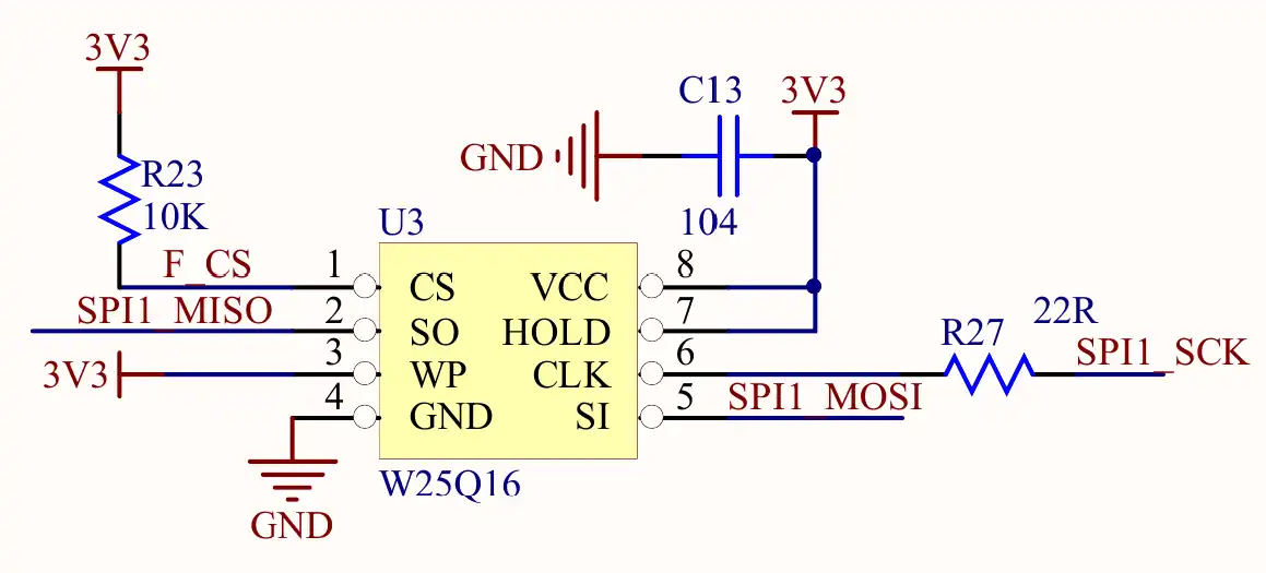
Note that the WP (Write Protect) pin is active Low pin, so it must be pulled HIGH when you want to modify the flash, and pulled LOW when you want to disable the modification.
The connections shown above are for the Single SPI mode, not for Dual or Quad modes.
CubeMX Setup
We will enable the SPI in Full Duplex master mode. The configuration is shown below.
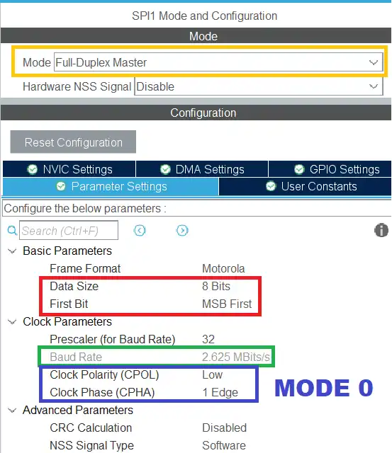
The Data width is set to 8 bits and the data should be transferred as the MSB first. The prescaler is set such that the Baud Rate is around 2.5 Mbits/sec.
According to the datasheet of the W25Q Flash, the SPI Mode 0 and Mode 3 are supported. Below is the image from the datasheet.
In the SPI configuration, we keep the Clock Polarity (CPOL) low and the Clock Phase (CPHA) to 1 edge. Here 1 edge means that the data will be sampled on the first edge of the clock. And when the CPOL is Low, the first edge is the rising edge. Basically we are using the SPI Mode 0.
In Full duplex Mode, SPI uses 3 pins, MOSI, MISO and CLK. We need to set one more pin as output so to be used as the Chip Select (CS) Pin.
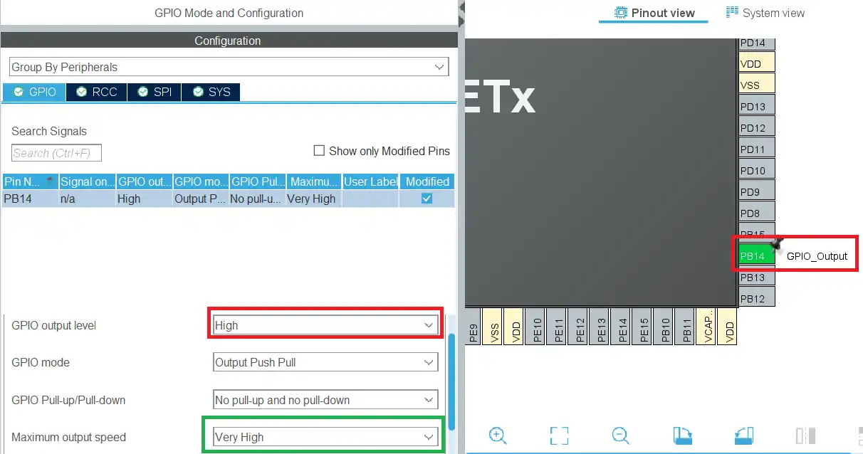
The Pin PB14 is set as the CS pin. The initial output level is set to HIGH. This is because the pin needs to be pulled low in order to select the slave device, so we keep it high initially to make sure the slave device isn’t selected. The Output speed is set to Very High because we might need to select and unselect the slave at higher rate.
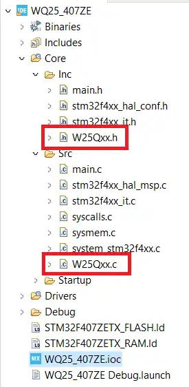
We created separate library files for the device. Today we will simply update the code in these files itself.
The files are: W25Qxx.c file in the src directory and W25Qxx.h file in the Inc directory.
Let’s Write the Code
We will write separate functions for Read and FastRead the data from the memory. I will explain both the commands and we will also take care of the situation, where we might need to change things for bigger sized memories (Typically above and including 256 Mb).
Let’s start with the Read operation.
Read Command
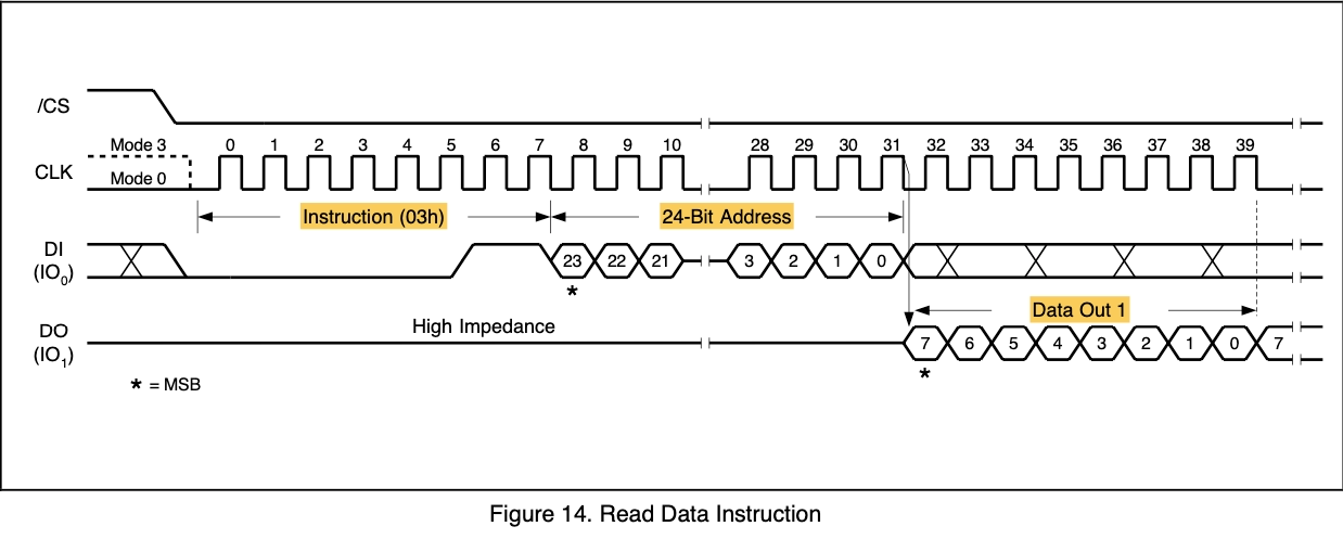
The Read Data instruction allows one or more data bytes to be sequentially read from the memory. The instruction is initiated by driving the CS pin low and then shifting the instruction code “03h” followed by a 24-bit address (A23-A0) / 32-bit address (A32-A0) into the DI pin. After the address is received, the data byte of the addressed memory location will be shifted out on the DO pin with most significant bit (MSB) first. The address is automatically incremented to the next higher address after each byte of data is shifted out allowing for a continuous stream of data. This means that the entire memory can be accessed with a single instruction as long as the clock continues. The instruction is completed by driving CS high.
Below is the image showing the Read Instruction Sequence.
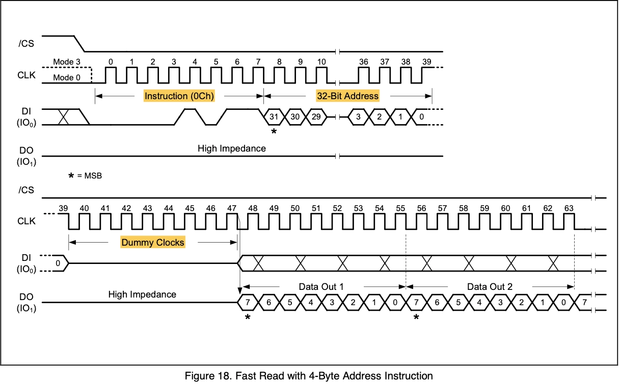
Just like Read command, there is another command to Read Data in the devices whose memory address can be 32bit wide.
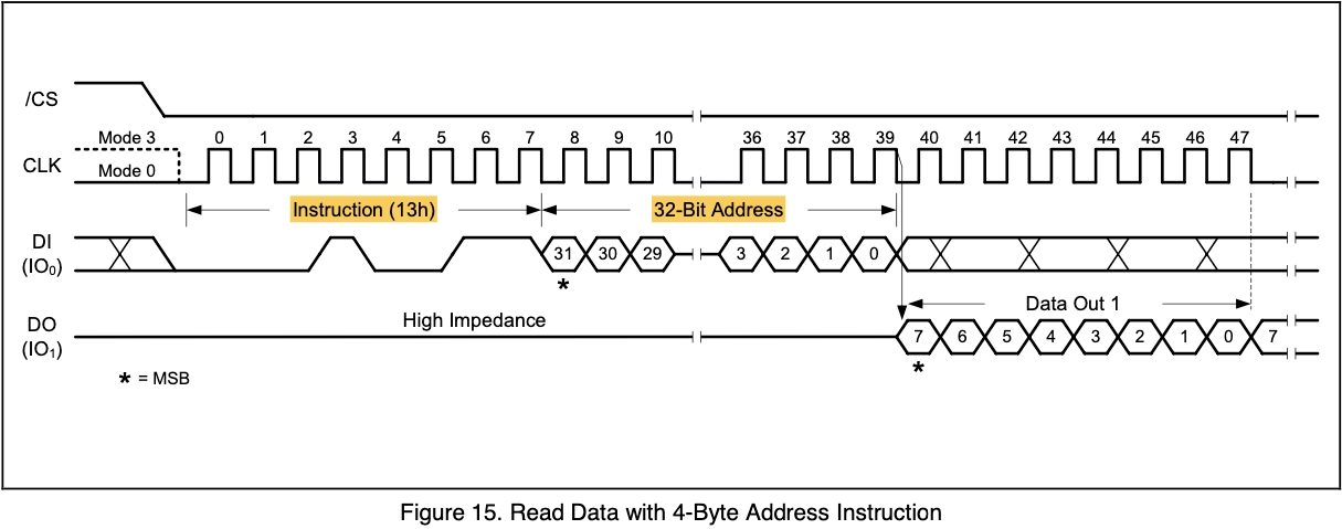
Although we can still use the regular Read command (0x03), but then we have to write separate code for the 24bit and 32 memory addresses. It’s better that we use the separate instruction itself.
The Read Data with 4-Byte Address instruction is similar to the Read Data (03h) instruction. Instead of 24- bit address, 32-bit address is needed following the instruction code 13h. No matter the device is operating in 3-Byte Address Mode or 4-byte Address Mode, the Read Data with 4-Byte Address instruction will always require 32-bit address to access the entire memory.
We write a function to Read the data from the memory.
define variables
We will start with defining some variables.
void W25Q_Read (uint32_t startPage, uint8_t offset, uint32_t size, uint8_t *rData)
{
	uint8_t tData[5];
uint32_t memAddr = (startPage*256) + offset;The parameters are as follows:
- @startPage is the page number where we want to start the Read fro. It can vary between 0 to (NUM_BLOCKS*256)-1.
- @offset is the offset in the start page. It can vary between 0 to 255, since there are 256 bytes in a page.
- @size is the amount of data we want to read (in Bytes).
- @rData is the pointer to the array where the received data will be stored.
In the function, we first define an array (tData) to send the instruction and address to the device. The instruction is 1 byte long, whereas the address can be 24/32 bit wide, hence 3/4 bytes long. In total we have the 4/5 bytes to send. This is why the tData is defined to hold 5 bytes (maximum in above scenario).
Then we calculate the memory Address (The byte address) from where we want to start the Read.
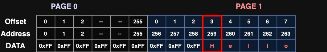
There are 256 bytes in 1 page, so the page number is multiplied with 256. Then we add it to the offset.
For example, if we want to read from PAGE 1 at an offset of 3, according to the formula, the memAddr = (1*256)+3 = 259. Basically we have to start reading form 259th byte, this is shown below.
Prepare the command
Now we will prepare the command to be sent to the device. In total we have to send the Read instruction and the 24/32 bit memory address.
	if (numBLOCK<512)   // Chip Size<256Mb
	{
		tData[0] = 0x03;  // enable Read
		tData[1] = (memAddr>>16)&0xFF;  // MSB of the memory Address
		tData[2] = (memAddr>>8)&0xFF;
		tData[3] = (memAddr)&0xFF; // LSB of the memory Address
}As I mentioned above, if the Flash memory is of lower size, the address would be 24 bit long. Basically if the device memory is lower than 256Mbits, the memory address would be 24 bit.
We will first copy the Read instruction into the array, and then copy the 24 bit address by splitting it into 3 bytes, with MSB (Most Significant Byte) to be sent first.
So totally we are sending 4 bytes of command in case of the memories with 24 bit address.
If the Flash memory size is 256MBits or more, we need to send 32 bit memory address. This is shown below.
	else
	{
		tData[0] = 0x13;  // Read Data with 4-Byte Address
		tData[1] = (memAddr>>24)&0xFF;  // MSB of the memory Address
		tData[2] = (memAddr>>16)&0xFF;
		tData[3] = (memAddr>>8)&0xFF;
		tData[4] = (memAddr)&0xFF; // LSB of the memory Address
}We do the same operation of copying the instruction and 32 bit address by splitting it into 4 bytes.
Transmit the command and Receive the Data
Now we have prepared the command, so it’s time to send it.
	csLOW();  // pull the CS Low
	if (numBLOCK<512)
	{
		SPI_Write(tData, 4);  // send read instruction along with the 24 bit memory address
	}
	else
	{
		SPI_Write(tData, 5);  // send read instruction along with the 32 bit memory address
	}

	SPI_Read(rData, size);  // Read the data
	csHIGH();  // pull the CS High
}- Pull the CS Low before sending the command.
- We use the
SPI_Writefunction to send the number of command bytes as per the 24/32 bit device address. - The function
SPI_Readwill be used to Receive the data sent by the device.- The number of bytes received will be decided by the size variable.
- The received data will be stored in the rData array.
- After the reception is over, pull the CS Pin High to release the device.
FastRead Command
The Fast Read instruction is similar to the Read Data instruction except that it can operate at the highest possible frequency.
The Fast Read is accomplished by adding eight “dummy” clocks after the 24/32-bit address. The dummy clocks allow the devices internal circuits additional time for setting up the initial address.
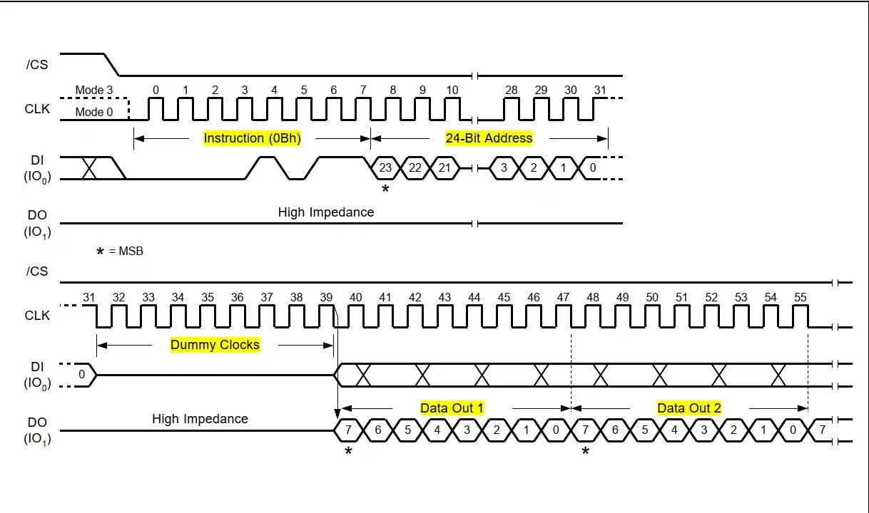
Just like the FastRead instruction, there is Fast Read with 4-Byte Address. It is similar to the Fast Read instruction except that it requires 32-bit address instead of 24-bit address. No matter the device is operating in 3-Byte Address Mode or 4-byte Address Mode, the Read Data with 4-Byte Address instruction will always require 32-bit address to access the entire memory.
We will write the similar function as Read, with the addition of dummy clocks in the command. Below the code shows the Fast Read function.
void W25Q_FastRead (uint32_t startPage, uint8_t offset, uint32_t size, uint8_t *rData)
{
	uint8_t tData[6];
	uint32_t memAddr = (startPage*256) + offset;

	if (numBLOCK<512)   // Chip Size<256Mb
	{
		tData[0] = 0x0B;  // enable Fast Read
		tData[1] = (memAddr>>16)&0xFF;  // MSB of the memory Address
		tData[2] = (memAddr>>8)&0xFF;
		tData[3] = (memAddr)&0xFF; // LSB of the memory Address
		tData[4] = 0;  // Dummy clock
	}
	else
	{
		tData[0] = 0x0C;  // Fast Read with 4-Byte Address
		tData[1] = (memAddr>>24)&0xFF;  // MSB of the memory Address
		tData[2] = (memAddr>>16)&0xFF;
		tData[3] = (memAddr>>8)&0xFF;
		tData[4] = (memAddr)&0xFF; // LSB of the memory Address
		tData[5] = 0;  // Dummy clock
	}

	csLOW();  // pull the CS Low
	if (numBLOCK<512)
	{
		SPI_Write(tData, 5);  // send read instruction along with the 24 bit memory address
	}
	else
	{
		SPI_Write(tData, 6);  // send read instruction along with the 32 bit memory address
	}

	SPI_Read(rData, size);  // Read the data
	csHIGH();  // pull the CS High
}You can see the function above is exactly the same, except the last command byte is set to 0. This is to provide the dummy clock to the device. Because of this extra command byte we are sending one extra byte to the device, so 5 bytes for memories with 24 bit address and 6 bytes for memories with 32 bit address.
Result
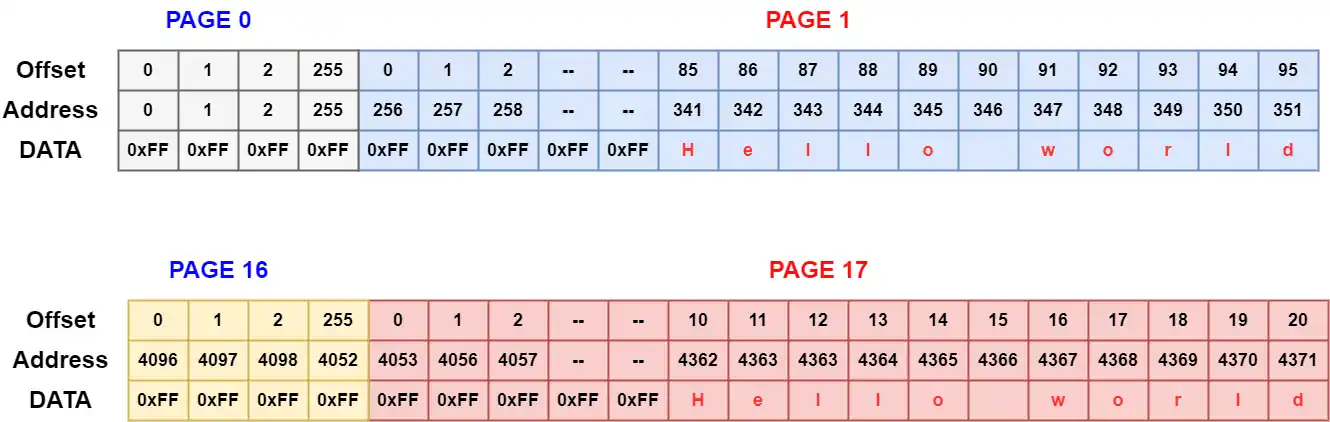
I have stored the data “Hello world” at 2 different locations in the memory. Both locations are in different sectors, sector 0 (page0 to page15) and sector 1 (page16 to page31).
I intentionally chose the different sectors, to demonstrate that we can perform continuous read even between the sectors. The image below shows how the data is placed and what is the memory address for the corresponding byte.
We will Read the data using 5 different statements and I will show the result of each one of them. The statements are as follows
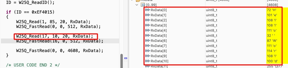
W25Q_Read(1, 85, 20, RxData); // Read 20 bytes from Page 1 Offset 85
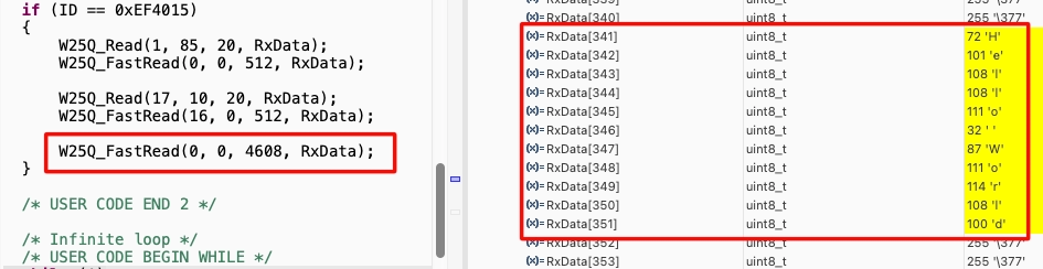
W25Q_FastRead(0, 0, 512, RxData); // Read 512 bytes (2 Pages) from the start of Page 0
W25Q_Read(17, 10, 20, RxData); // Read 20 bytes from Page 17 Offset 10
W25Q_FastRead(16, 0, 512, RxData); // Read 512 bytes (2 Pages) from the start of Page 16
W25Q_FastRead(0, 0, 4608, RxData); // Read 4608 bytes (18 Pages) from the start of Page 0Let’s see the output of the first statement, i.e. W25Q_Read(1, 85, 20, RxData); // Read 20 bytes from Page 1 Offset 85
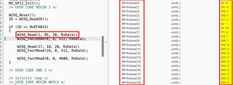
The image above shows that we received the data, “Hello world”, at the beginning of the RxData buffer. This is as expected because we read from the offset of 85. This is where the data is actually stored in the memory.
If we Read the data from the beginning of the memory, i.e. from page 0 offset 0, we should get data in the RxData buffer at an offset of 341 (1×256 + 85). This is the actual position of the data from the start of the memory as shown in the figure main memory map.
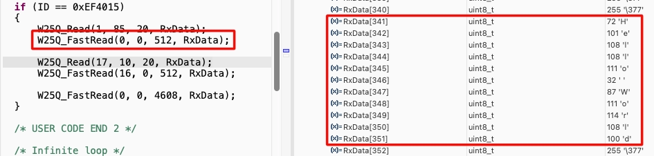
Here we are performing the Fast Read operation to read 512 bytes from the start of the memory. W25Q_FastRead(0, 0, 512, RxData); We have received the data in the RxData buffer at an offset of 341.
The next statement reads the data from second location, which is stored on page 17 at an offset of 10. The statement W25Q_Read(17, 10, 20, RxData); Reads the data from the same location, so we should get the data at the beginning of the RxData buffer itself.
As shown in the image above, we received the data in the beginning of the RxData buffer itself.
The next statement reads the data from the start of the page 16. This time we should get data in the RxData buffer at an offset of 266 (1×256 + 10). This is the actual position of the data from the start of the page 16 as shown in the figure main memory map
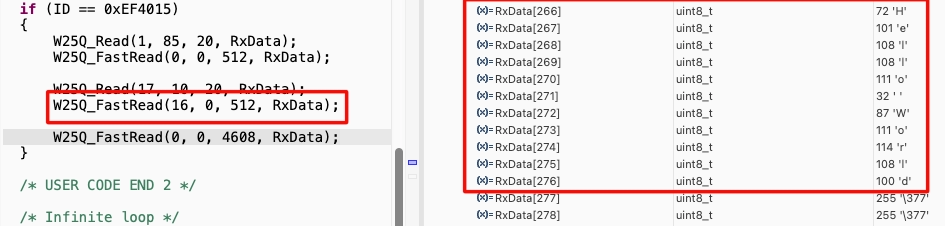
The statement W25Q_FastRead(16, 0, 512, RxData); Reads 512 bytes of data from the start of the page 16, so we received the data at an offset of 266 in the RxData buffer.
Now we will read both the data locations from the start of the memory. This demonstrates that multiple sectors can be read with a simple read command and we just need to set the size according to the number of bytes we want to read.
The statement W25Q_FastRead(0, 0, 4608, RxData); Reads 4608 bytes from the start of the memory. Basically we are reading 18 pages in total, which reads across one full sector [sector 0 (page0 to page15) and sector 1 (page16 to page31)].
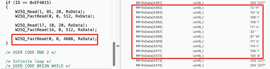
As shown above, the first image shows the first data which is at an offset of 341 from the start. The second data is at an offset of 4362 from the start. This is as per the locations shown in the figure main memory map.
STM32 W25Q Flash Tutorials Series
W25Q Flash Series Part 3 – How to Erase Sectors
W25Q Flash Series Part 4 – How to Program Pages
W25Q Flash Series Part 5 – how to update sectors
W25Q Flash Series Part 6 – Integers floats and 32bit Data
W25Q Flash Series Part 7 – QUADSPI Write, Read, Memory Mapped mode
W25Q Flash Series Part 8 – QUADSPI External Loader
W25Q Flash Series Part 9 – SPI Flash Loader


In read function i get only 255 value constantly
Moi aussi, est ce que vous avez pu le régler svp ??
Thank you for your Contribution. It has helped me a lot. But could you please tell me in several specification there is Address is written as Axh, Bxh, Cxh, 0xh . I could not understand the notation here. Could you tell me what would be this address? what does x stand for?
‘I have stored the data “Hello world” at 2 different locations in the memory…’
How do you write it, I don’t see the function in your code
check out PART 4
Thank you. I have checked, and do step by step as your article. But data received only 0xff, 0xff, 0xff… What happen, do you have suggest for me
Before that, I read the ID of W25Q exactly as described in the datasheet, so the connection is OK, right?
Which memory are you using? and how many bytes are you writing?
I used W25Q128FVSG
I define:
uint8_t RxData[4608];
uint8_t TxData[30] = {1,2,3,4,5,6,7,8,9};
In main function, i call write/read flash like below:
W25Q_Write_Page(0, 250, 9, TxData);
W25Q_Read(0, 250, 20, RxData);
And the result the RxData is 0xff, 0xff, 0xff,.. not same as TxData
I don’t know what’s happen, hope you have advice for me, thank you very much.
Is it able to read the ID correctly ?
shield your code inside the correct ID
if (ID == 0x123456)
{
write_page
read_page
}
also define smaller array if you are using just 9 bytes of data. It takes time to update the data in the live expression, so wait there… don’t exit the debugger instantly.
Thank you for your advice, i already resolved it. My mistake is WP pin do not pulled up when write data
Thank so much