Home ▸ STM32 Tutorials ▸
Updated On: April 12, 2026
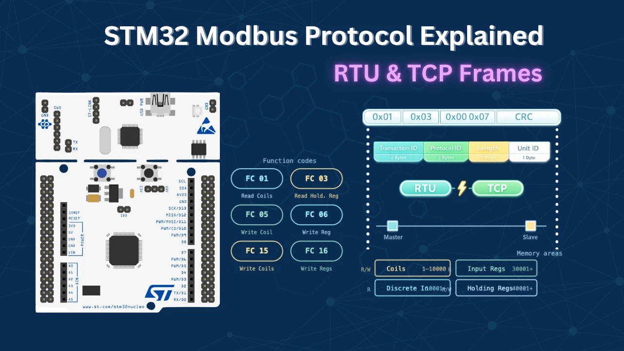
Master Writes Multiple Coils and Registers
This is another tutorial in the Modbus series and today we will see how to use the STM32 as the master, which will Write multiple coils and Holding Registers. I have already covered writing single coil and Register in This tutorial.
Basically we will be covering the function codes FC15 and FC16 in this tutorial.
We will continue with where we left in the previous tutorial. You must see it first as I am going to skip few explanation in this tutorial.
VIDEO TUTORIAL
You can check the video to see the complete explanation and working of this project.
The Connection
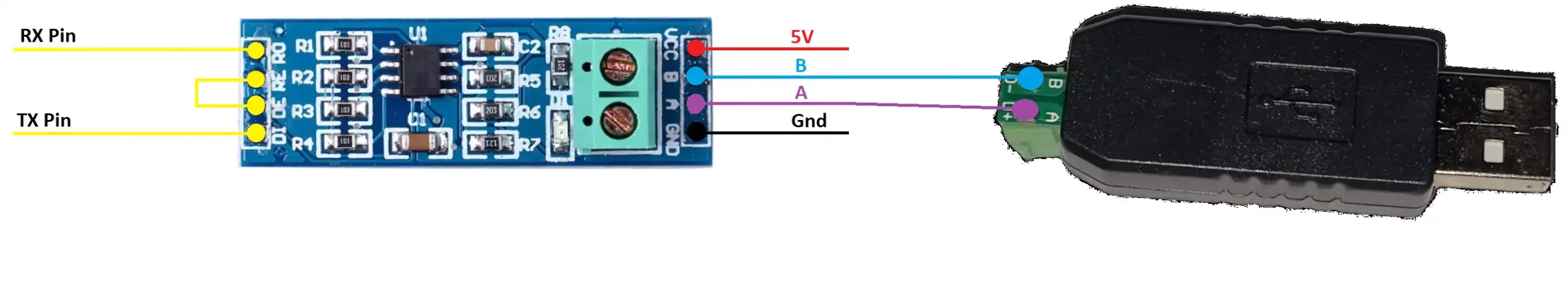
Below is the connection diagram of the module with the STM32F103C8 controller.
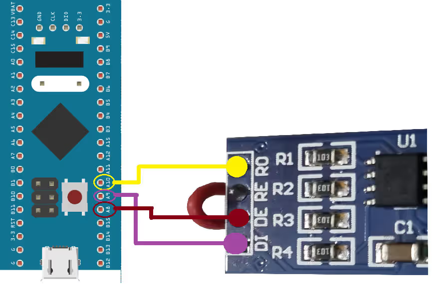
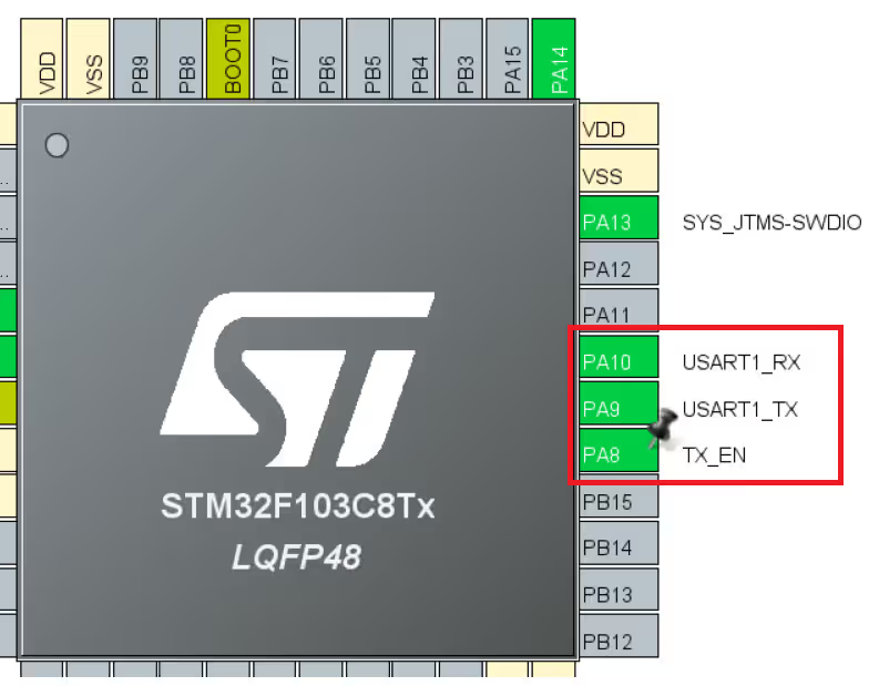
As shown above, The RO pin is connected to the PA10 (UART1 RX) and DI pin is connected to the PA9 (UART1 TX).
The RE and DE are connected together with the pin PA8, which we have set as the output in the MCU.
The CubeMX configuration is shown below
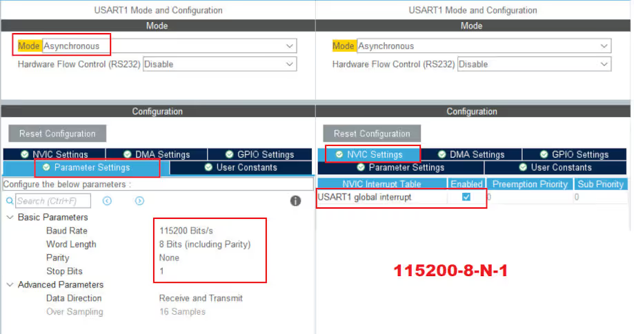
The UART1 is configured to it’s default setup with the baud rate of 115200 and 8-N-1. Also I have enabled the interrupt to receive the data from the second controller.
The pin PA8 is set as output and I have renamed it to the TX_EN pin.
In this tutorial the STM32 will act as a master and since I don’t actually have a slave device, I am going to use a software in the computer that will make the computer to act as a slave device.
The communication will take place using the RS485 standard. STM32 is connected to the RS485 to TTL converter and the computer is connected via the RS485 to USB converter.
This is it for the connection, let’s see the code now.
The Slave Software
As I mentioned above I am going to use a software so the computer can act as a slave device.
The software can be downloaded from https://www.simplymodbus.ca/RTUslave.htm
Some components of the software are explained below
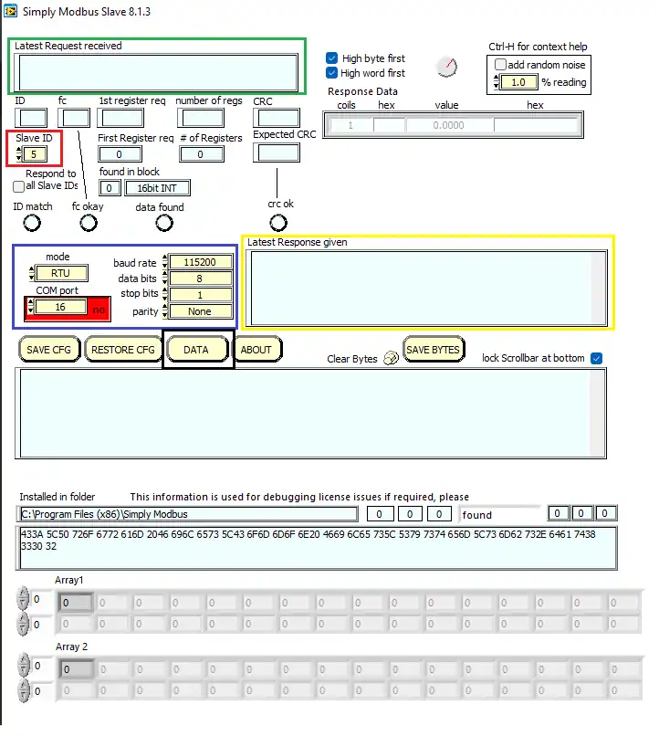
- We have the Slave ID, which we can set manually.
- The window in the Green box shows the request sent by the slave (in hex format)
- The Blue box is the Port configuration. make sure that the master and slave are configured similarly
- The yellow box shows the data sent by the slave (in hex format)
Since this is a slave device, it already have the memory areas (coils and registers). We can access them by clicking the DATA button (in Black box)
Below is the image of the registers and coils available
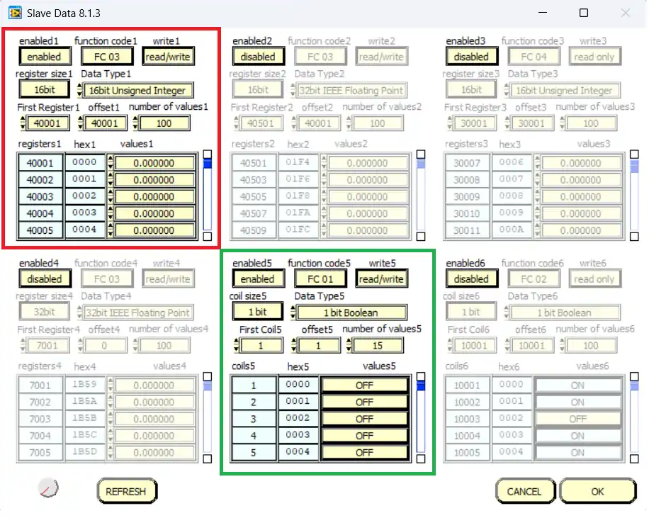
Here we are only concerned about the Red box and Green box
- I have enabled the function code 3 and 1 i.e Reading Holding Registers and coils.
- This is because the software specifically don’t have the function codes 15 and 16
- But since I have enabled the Read/Write, we can use the FC 15 and 16.
- The memory size for the coils is 1 bit and that for the Registers is 16 bit.
Some insight into the code
Writing Multiple Coils
First We will create a function to send the data via the UART. The modbus module need to be put in the transmit mode before sending the data.
uint8_t RxData[10];
uint8_t TxData[11];

void sendData (uint8_t *data)
{
  HAL_GPIO_WritePin(TX_EN_GPIO_Port, TX_EN_Pin, GPIO_PIN_SET);
  HAL_UART_Transmit(&huart2, data, 11, 1000);
  HAL_GPIO_WritePin(TX_EN_GPIO_Port,TX_EN_Pin , GPIO_PIN_RESET);
}- Here I have first defined the RX and TX buffers.
- The
sendDatafunction will be used by the master to send the request to the slave device. - Here we will first pull the TX_EN pin (RE and DE Pins) High. This will put the module in the transmitter mode.
- Then we will send the data via the UART.
- After sending the data, we will again pull the TX_EN pin LOW, so to put the module in the receive mode.
The number of elements in the TxData buffer depends on how much data the master wants to write. Here I have defined the TxData with 11 elements.
The Data format
Before we actually send the request to the slave device, we need to prepare our TxData buffer.
The request pattern sent by the master to write multiple coils is shown in the picture below
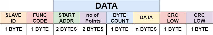
- Here the DATA field consists of the start address, the coil address where the modification begins
- The no of points, the number of coils master wants to modify
- The Byte count, the number of bytes master will be sending
- The DATA itself (for the coils)
The number of points and Byte count are different. Here in case of coils, the size of data for each coil is 1 Bit. We also know that the data can be only transferred in bytes.
So if the master wants to write upto 8 coils, it needs to send 1 byte of data. Similarly if the master wants to write upto 16 coils it needs to send 2 Bytes of data.
Even if the master wants to write 9 coils, it still need to send 2 bytes of data for the same.
The TxData Buffer
Below is the TxData buffer that the master will send to the slave.
TxData[0] = 0x05;  // slave address
TxData[1] = 0x0F;  // Force Multiple coils

TxData[2] = 0;  // coil address high
TxData[3] = 3;  // coil address low
//The coil address will be 00000000 00000011 = 3 + 1 = 4

TxData[4] = 0;  // no. of coils high
TxData[5] = 0x0F;  // no. of coils low
// Total no. of coils = 00000000 00001111 = 15 coils

TxData[6] = 2; // Byte count (15 coils would need 2 bytes)

TxData[7] = 0x35;  // Data for first 8 coils
TxData[8] = 0x74;  // Data for next 8 coils (actually 7 coils)

uint16_t crc = crc16(TxData, 9);
TxData[9] = crc&0xFF;   // CRC LOW
TxData[10] = (crc>>8)&0xFF;  // CRC HIGH

sendData(TxData);- Here we have the Function code 15 (0x0F) for writing multiple coils
- The TxData[2] and [3] represents the Start coil Address, which is set to 3
- This means the actual coil location in the slave will be at 4
- The TxData[4] and [5] represents the no. of coils master wants to write. It is set to 15 coils
- Since 15 coils would require 15 bits, the master needs to send 2 Bytes of data (TxData[6]).
- TxData[7] and [8] represents the actual 2 Bytes of data the master is going to send
- TxData[9] and [10] contains the CRC.
- Finally the sendData function will send the data to the slave.
The 2 Data bytes sent by the master will be received in the similar order by the slave device. Here in this example, the first byte, 0x35, will be used for the coils 4-11. And the second byte, 0x74, will be used for the coils 12-18.
The Result
Below is the image showing the data in the coils 4-18. I have also arranged the data in the Byte format indicating the actual data stored in the coils

As you can see above, the data stored in the coils is exactly what the master sent. The first Byte (0x35) is used for the coils 4-11 and the send Byte (0x74) is used for the coils 12-18.
The Video for the same can be found at the end of the post.
Writing Multiple Registers
The sendData function will be used to send the data to the slave device.
uint8_t RxData[10];
uint8_t TxData[15];

void sendData (uint8_t *data)
{
  HAL_GPIO_WritePin(TX_EN_GPIO_Port, TX_EN_Pin, GPIO_PIN_SET);
  HAL_UART_Transmit(&huart2, data, 15, 1000);
  HAL_GPIO_WritePin(TX_EN_GPIO_Port,TX_EN_Pin , GPIO_PIN_RESET);
}- Here I have first defined the RX and TX buffers.
- The
sendDatafunction will be used by the master to send the request to the slave device. - Here we will first pull the TX_EN pin (RE and DE Pins) High. This will put the module in the transmitter mode.
- Then we will send the data via the UART.
- After sending the data, we will again pull the TX_EN pin LOW, so to put the module in the receive mode.
The number of elements in the TxData buffer depends on how much data the master wants to write. Here I have defined the TxData with 15 elements.
The Data format
Before we actually send the request to the slave device, we need to prepare our TxData buffer.
The request pattern sent by the master to write multiple Registers is shown in the picture below
- Here the DATA field consists of the start address, the Register address where the modification begins
- The no of points, the number of Registers master wants to modify
- The Byte count, the number of bytes master will be sending
- The DATA itself (for the Registers)
The number of points and Byte count are different. Here in case of Registers, the size of data for each Register is 16 Bit. We also know that the data can be only transferred in bytes.
So if the master wants to write 1 Register, it needs to send 16 bits i.e. 2 Bytes of Data. Similarly for 2 Registers, the master needs to send 4 Bytes. And for 3 Registers the master will send 6 Bytes and so on.
The TxData Buffer
Below is the TxData buffer that the master will send to the slave.
TxData[0] = 0x05;  // slave address
TxData[1] = 0x10;  // Preset multiple Registers

TxData[2] = 0;  // Register address high
TxData[3] = 0;  // Register address low
//The coil address will be 00000000 00000000 = 0 + 40001 = 40001

TxData[4] = 0;  // no. of Registers high
TxData[5] = 0x03;  // no. of Registers low
// Total no. of Registers = 00000000 00000011 = 3 Registers

TxData[6] = 6; // Byte count (3 Registers would need 6 bytes (2 bytes per register))

TxData[7] = 0x12;  // Data High for first Register
TxData[8] = 0x34;  // Data low for first Register
TxData[9] = 0x56;  // Data High for 2nd Register
TxData[10] = 0x78;  // Data low for 2nd Register
TxData[11] = 0xab;  // Data High for 3rd Register
TxData[12] = 0xcd;  // Data low for 3rd Register

uint16_t crc = crc16(TxData, 13);
TxData[13] = crc&0xFF;   // CRC LOW
TxData[14] = (crc>>8)&0xFF;  // CRC HIGH

sendData(TxData);- Here we have the Function code 16 (0x10) for writing multiple Registers
- The TxData[2] and [3] represents the Start Register Address, which is set to 0
- This means the actual Register location in the slave will be at 40001
- The TxData[4] and [5] represents the no. of Registers master wants to write. It is set to 3 Registers
- Since 3 Registers would require 48 bits, the master needs to send 6 Bytes of data (TxData[6]).
- TxData[7] to TxData[12] represents the actual 6 Bytes of data the master is going to send
- TxData[13] and [14] contains the CRC.
- Finally the sendData function will send the data to the slave.
The 6 Data bytes sent by the master will be received in the similar order by the slave device, 2 bytes for each Register.
This means the TxData[7] and [8] will be used by the Register at the location 40001, TxData[9] and [10] will be used by the Register at 40002 and TxData[11] and [12] will be used by the Register at 40003.
The Result
Below is the image showing the Registers in the Slave device.
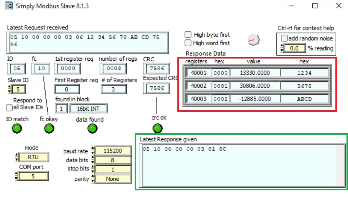
- Here the RED box represents the Registers modified in the slave device.
- The Register at 40001 contains the value 0x1234, which were the first 2 bytes of the Data master sent.
- similarly the Registers at 40002 and 40003 contains the other 4 Bytes.
The GREEN box contains the slave response. It consists of:
- The slave ID
- The Function code
- The Start Register Address
- The number of Registers written
- The CRC
STM32 Modbus RTU Tutorial Series

Modbus #1. STM32 Master Reads Holding and Input Registers

Modbus #2. STM32 Master Reads Coils and inputs

Modbus #3. STM32 Master Writes single Coil and Holding Register

Modbus #4. STM32 as Slave || Read Holding and Input Registers

Modbus #5. STM32 as Slave || Read Coils and Inputs

Modbus #6. STM32 as Slave || Write Registers

Modbus #7. STM32 as Slave || Writing Coils

Subscribe
Login
0 Comments
Newest
