Updated On: February 9, 2026
STM32 Master – slave communication over LIN Bus
This is the 9th tutorial in the series on the UART peripheral of STM32 Microcontrollers. In this series we will cover different ways of transmitting and receiving data over the UART protocol. We will also see different UART modes available in the STM32 microcontrollers and how to use them.
In the previous parts of this series, we covered the basics of the LIN (Local Interconnect Network) protocol and how it can be implemented on STM32 using the UART peripheral and a LIN transceiver. While understanding frame structure and configuration is important, the real value of LIN comes from seeing actual master–slave communication in action.
In this part of the tutorial, we build a complete LIN master and LIN slave setup using two STM32 boards. You’ll see how the master sends different LIN commands based on user input, how the slave interprets those frames to control outputs or return data, and how both sides handle frame transmission and reception. This example demonstrates practical, bidirectional LIN communication and shows how LIN can be used in real embedded and automotive-style applications.
Wiring Connection between Master and Slave
This tutorial is a continuation of the previous one, so we will just add few more things to the connection shown previously. Below is the image showing the connection diagram for this tutorial.
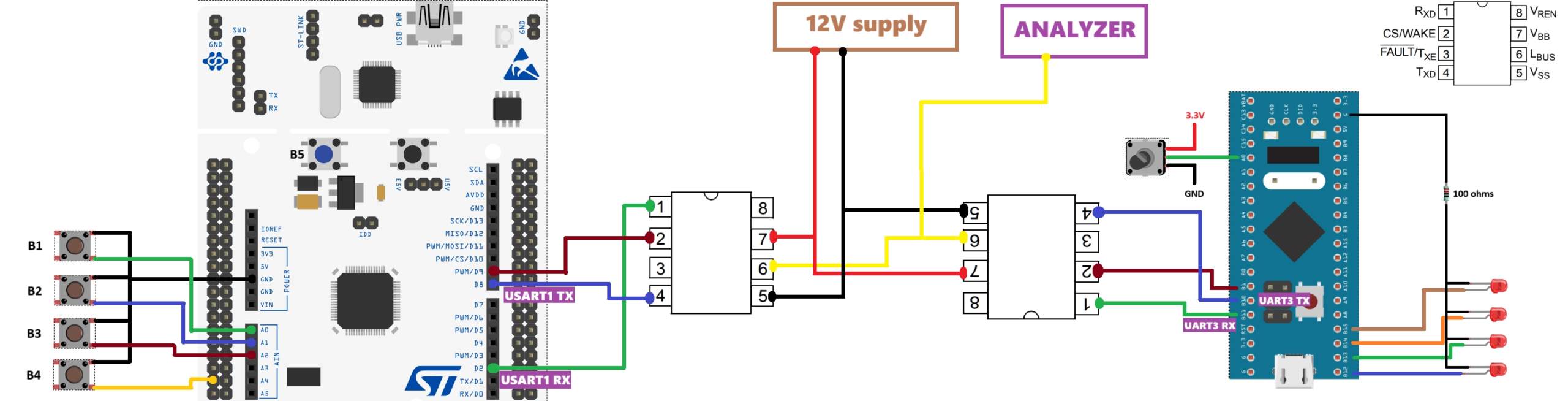
As shown in the setup above, the LIN master MCU is connected to a total of five buttons—four external buttons and one on-board user button. The external buttons are connected to pins PA0, PA1, PA4, and PC2, while the on-board user button is connected to PC13.
The four external buttons are used to control four LEDs on the LIN slave MCU, with each button triggering a specific command from the master. The on-board button (B5) is used to request ADC data from the slave. Whenever a button is pressed, the master sends a corresponding LIN command, which is received, decoded, and processed by the slave.
On the slave side, the four LEDs are connected to pins PB12, PB13, PB14, and PB15. A potentiometer is connected to PA0, and its value is read using the ADC. When requested by the master, the slave sends the ADC data back over the LIN bus as part of its response frame.
Configuring the LIN Master Node
In this setup, the STM32F446 is configured as the LIN master device. The master is responsible for initiating communication on the LIN bus by sending LIN frames and controlling when data is exchanged with the slave nodes.
CubeMX Configuration
Below is the image showing the configuration of the UART in the Lin mode.
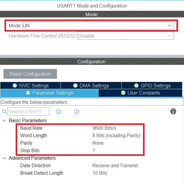
The USART1 is configured in the LIN mode. The LIN protocol supports the transfer up to the baud rate of 200 Kbps, but here I am using 9600 bps. The data size is set to 8 bits with no parity and 1 stop bit.
We also need to set a GPIO pin as the output. This will be used as the CS pin for the transceiver.
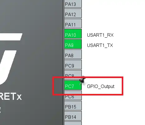
Here I am setting the pin PC7 as the output pin.
We also need to configure the input pins for the buttons. The buttons on the master will control the LEDs on the slave device.
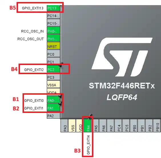
As shown in the image above, I have set 5 different pins as the EXTI pins. The pins are chosen such that there is no conflict between the external interrupts.
All the buttons are connected between the MCU pin and the ground. Therefore when the button is pressed, respective pin is pulled low to the ground.
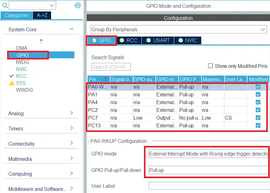
To ensure that the pin is pulled low to the ground only after the button is pressed, we need to enable the pull up for all the pins.
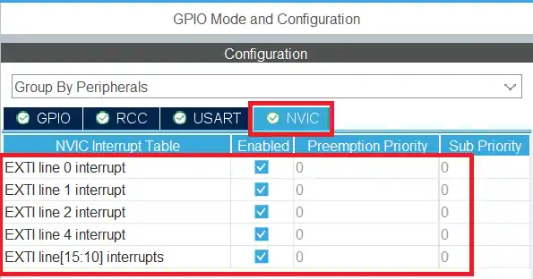
Finally we need to enable the interrupts for all the EXTI pins. This can be done in the NVIC Tab.
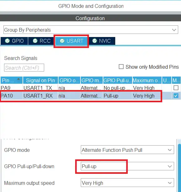
Since the master is also going to receive the data, we need to make sure that the UART RX pin is pulled high for the master. This can be done in the USART tab as shown below.
HAL Code for the LIN Master
When either of the button is pressed, an interrupt will trigger and the External Interrupt callback is called.
int B1=0, B2=0, B3=0, B4=0, B5=0, transmit=0;
void HAL_GPIO_EXTI_Callback(uint16_t GPIO_Pin)
{
	if (GPIO_Pin == GPIO_PIN_0)
	{
		B1 = transmit = 1;
		B2 = B3 = B4 = B5 = 0;
	}
	else if (GPIO_Pin == GPIO_PIN_1)
	{
		B2 = transmit = 1;
		B1 = B3 = B4 = B5 = 0;
	}
	else if (GPIO_Pin == GPIO_PIN_4)
	{
		B3 = transmit = 1;
		B1 = B2 = B4 = B5 = 0;
	}
	else if (GPIO_Pin == GPIO_PIN_2)
	{
		B4 = transmit = 1;
		B1 = B2 = B3 = B5 = 0;
	}
	else if (GPIO_Pin == GPIO_PIN_13)
	{
		B5 = transmit = 1;
		B1 = B2 = B3 = B4 = 0;
	}
}Inside the callback we will check which pin called this callback. Then set the respective variable and reset the other variables. We will also set the transmit variable with each button pressed, so that the master can transmit the data on the LINBus.
We will take care of the data transmission part inside the while loop.
Inside the while loop, we will only transmit the data if the transmit variable is set.
while (1)
{
if (transmit == 1)
{
HAL_Delay(300);
TxData[0] = 0x55; // sync field
TxData[1] = pid_Calc(0x34);
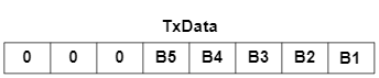
TxData[2] = (B1<<0) | (B2<<1) | (B3<<2) | (B4<<3) | (B5<<4);
TxData[3] = checksum_Calc(TxData[1], TxData+2, 1); //lin 2.1 includes PID, for line v1 use PID =0The delay (300ms) is used to prevent the button debouncing.
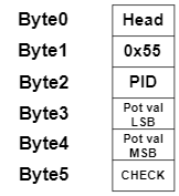
The TxData array will contain the Linbus frame to be transmitted. It contains the header field, the Sync field, The PID, the Data byte and the checksum byte.
The Data byte is the combination of the value of all the variables defined for the buttons. We basically use the button values as a single bit and combine them in the data byte.
Now the TxData buffer is prepared so we will send it via the Linbus.
		  HAL_GPIO_WritePin(CS_GPIO_Port, CS_Pin, GPIO_PIN_SET);
		  HAL_Delay(100);
		  HAL_LIN_SendBreak(&huart1);
		  HAL_UART_Transmit(&huart1, TxData, 4, 1000);
		  HAL_GPIO_WritePin(CS_GPIO_Port, CS_Pin, GPIO_PIN_RESET);
transmit = 0;To send the LIN frame, the master will first set the CS pin. This will enable the transmitter in the LIN Transceiver. After that, the master will send the break field, followed by the TxData array.
Once the entire frame is transmitted, the master will reset the CS pin to disable the transmitter. This will prevent any data conjunction on the Linbus when the slave is transmitting the data.
When the button 5 is pressed, the slave will transmit the data containing ADC value. The master shall be prepared to receive this data.
		  if (HAL_UART_Receive(&huart1, RxData, 6, 500) == HAL_OK)
		  {
			  uint8_t checksum = checksum_Calc(RxData[2], RxData+3, 2);
			  if (checksum == RxData[5])
			  {
				  ADC_DATA = RxData[3] | (RxData[4]<<8);
			  }
		  }
	  }
}The HAL_UART_Receive is used to receive the 6 bytes of data in the blocking mode. I have used a timeout of 500ms. If the 6 bytes data is not received within this time, the function will timeout and the if condition will fail, otherwise we will have a valid data from the slave.
If all the 6 bytes are received, we will first calculate the checksum to verify if the data received is correct. The 12 bit ADC data is sent by the slave in 2 separate bytes. We will combine these bytes to make a single 12 bit data.
Configuring the LIN Slave Node
I am going to use the STM32F103 as the slave device.
CubeMX Configuration
The basic configuration will remain the same, so we will just configure the additional pins and peripherals here.
Let’s start with adding the LEDs to this configuration. This is shown below.
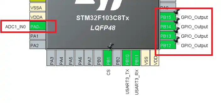
The 4 LEDs are connected to the pins PB12, PB13, PB14 and PB15. These LEDs will be controlled by the buttons on the master. We also have the potentiometer connected to the slave, which will be read using the ADC pin PA0.
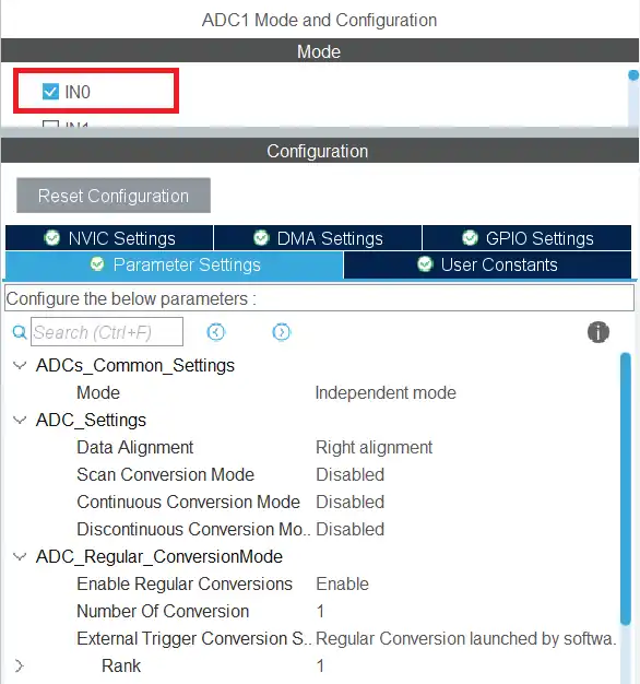
I have enabled the channel 0 of the ADC 1. The ADC is configured with the default setup.
HAL Code for the LIN Slave
Most of the code remains the same as we covered in the previous tutorial. The slave receives the data via the UART in the interrupt mode, checks the data validity, and if the data is valid, it extracts the actual data bytes from the received frame.
Here we will just cover the main function.
  while (1)
  {

	  if (isDataValid == 1)
	  {
		  for (int i=0; i<numDataBytes; i++)
		  {
			  Data[i] = RxData[i+3];
}Here we will check if the isDataValid variable is set to 1. If it is, then we will copy the received data from the RX buffer to the Data buffer. The master sent only 1 Data byte and it contains the information about which button is pressed.
Based on the this information, we will set the respective LED.
		  HAL_GPIO_WritePin(GPIOB, GPIO_PIN_12, (Data[0]&0x01));
		  HAL_GPIO_WritePin(GPIOB, GPIO_PIN_13, ((Data[0]>>1)&0x01));
		  HAL_GPIO_WritePin(GPIOB, GPIO_PIN_14, ((Data[0]>>2)&0x01));
HAL_GPIO_WritePin(GPIOB, GPIO_PIN_15, ((Data[0]>>3)&0x01));The 4 buttons are used to control 4 LEDs on the slave. The fifth button however requests the ADC data from the slave.
		  if (((Data[0]>>4)&0x01) == 1)
		  {
			  HAL_ADC_Start(&hadc1);
			  HAL_ADC_PollForConversion(&hadc1, 100);
			  uint16_t adcVal = HAL_ADC_GetValue(&hadc1);
HAL_ADC_Stop(&hadc1);We first check is the fifth button is pressed. If it is, the slave will start reading the ADC value. Here I am using the simple polling method to read the ADC value and it is stored in the adcVal variable. The STM32F103C8 has the 12 bit ADC resolution by default, hence we need to define a 16 bit variable to store the value.
Now that we have the ADC value, we will send it via the Linbus. To do that, we first need to prepare the Lin frame to be transmitted.
			  uint8_t TxData[10];
			  TxData[0] = 0x55;  // sync field
			  TxData[1] = pid_Calc(0x35);
			  TxData[2] = adcVal&0xFF;
			  TxData[3] = (adcVal>>8)&0xFF;
TxData[4] = checksum_Calc(TxData[1], TxData+2, 2); //lin 2.1 includes PID, for line v1 use PID =0The TxData array will contain the lin frame. We will store the sync filed, followed by the PID, the actual Data bytes and finally the checksum byte.
Here I am using a separate ID for the slave, 0x35. Since the ADC Data is 12 bit in size, we need to send it in 2 separate bytes, with the LSB being sent first.
We have the lin frame, so the next part is to transmit this frame via the UART.
			  HAL_GPIO_WritePin(CS_GPIO_Port, CS_Pin, GPIO_PIN_SET);
			  HAL_Delay(100);
			  HAL_LIN_SendBreak(&huart3);
			  HAL_UART_Transmit(&huart3, TxData, 5, 1000);
			  HAL_GPIO_WritePin(CS_GPIO_Port, CS_Pin, GPIO_PIN_RESET);
		  }
		  isDataValid = 0;
	  }
}To send the lin frame, the slave will first set the CS pin. This will enable the transmitter in the Lin Transceiver. After that, the slave will send the break field, followed by the TxData array.
Once the entire frame is transmitted, the slave will reset the CS pin to disable the transmitter. This will prevent any data conjunction on the Linbus when the master is transmitting the data.
Once all the processing is done, reset the isDataValid variable to 0. This will prevent this loop from running again until the next data is sent by the master.
Video Tutorial
STM32 LIN Protocol – Master & Slave Interaction (Part 3)
This video demonstrates a complete LIN master–slave communication setup using two STM32 boards. You’ll see how the LIN master sends different commands, how the slave processes them to control LEDs or return ADC data, and how bidirectional data exchange works over the LIN bus.
Watch the VideoConclusion
This part of the tutorial demonstrates how a complete LIN master–slave system can be built using STM32 and the UART peripheral. By combining proper frame construction, break generation, and interrupt-based reception, the master and slave are able to exchange commands and data reliably over the LIN bus. The example shows how real control tasks, such as LED switching and ADC data requests, can be handled using standard LIN communication principles.
Once this bidirectional communication flow is understood, it becomes easier to scale the system by adding more slave nodes or expanding the command set. This approach closely reflects how LIN is used in real automotive and industrial applications, making it a solid foundation for developing robust, low-cost networked embedded systems using STM32.
Browse More STM32 UART Tutorials
STM32 UART Part 3 – Receive Data in Blocking & Interrupt mode
STM32 UART DMA Receive: Normal & Circular Mode (HAL)
STM32 UART Idle Line: Receive Data via Interrupt & DMA
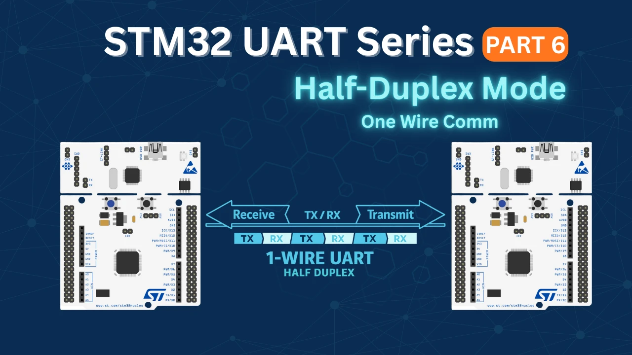
STM32 UART Part 6 – Half-Duplex Communication (Single-Wire Mode)
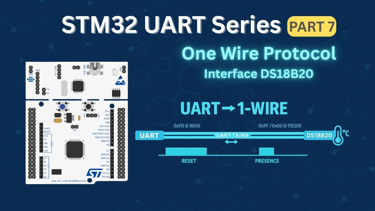
STM32 UART Part 7 – How to use one-Wire Protocol
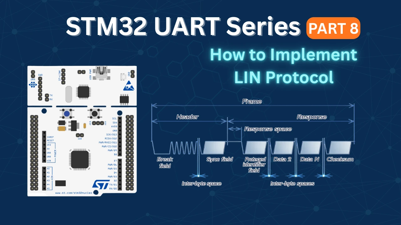
STM32 UART Part 8 – LIN Communication Tutorial
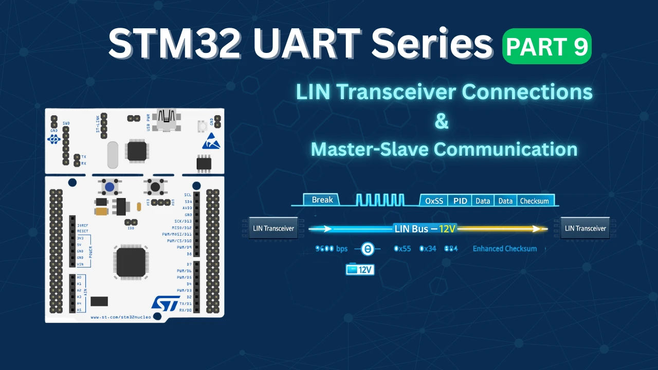
STM32 UART Part 9 – LIN Transceiver Connections & Master-Slave Communication
STM32 UART LIN Project Download
STM32 UART LIN FAQs


Did you get any example about the most real slave?
If you are preparing example on LIN communication, please do it like it is done in real cases. The master shall request the data from the Slave by sending header only. Then the slave shall response with the data only. Tbh your example is useless without this mechanism. Also receving fixed size data with polling mode is very bad way to do it.
Did you get any example about the most real slave?