Home ▸ STM32 Tutorials ▸
Updated On: March 23, 2026
How to Setup UART using Registers
This is yet another tutorial in the Register Based Series in STM32, and today we will see how can we setup the UART for Transmitting and receiving data.
This will be a simple setup, with no interrupts or DMA. We will simply receive and Transmit the data in the blocking mode. I will cover the Interrupts and DMA in the upcoming tutorials.
Let’s start with the PIN Setup for the UART
VIDEO TUTORIAL
You can check the video to see the complete explanation and working of this project.
PIN Configuration
I am going to use the UART 2, and the Pins that I need to setup are Pin PA2 for Tx and Pin PA 3 for Rx
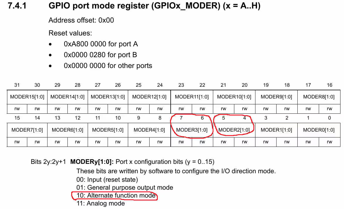
Since we are using the Pins for Alternate Function, we need to select the Alternate Function Mode in the MODE Register
RCC->AHB1ENR |= RCC_AHB1ENR_GPIOAEN;  // Enable GPIOA CLOCK

GPIOA->MODER 	 |= (2<<4);   // Bits (5:4)= 1:0 --> Alternate Function for Pin PA2
GPIOA->MODER |= (2<<6); // Bits (7:6)= 1:0 --> Alternate Function for Pin PA3- Here we will enable the Clock for the GPIOA Port
- Then select the Pins PA2 and PA3 in the Alternate Function mode
- This is done by writing ‘1 0’ (2) in the 4th and 6th positions.
Now the Pins are setup as the Alternate Functions, but we still need to choose which function exactly. For eg: Is it I2C, SPI or UART etc.
This can be done in the Alternate Function Register
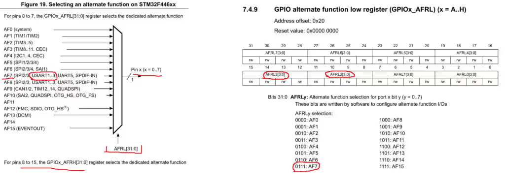
- Here First we have to look up for which alternate function is associated with the UART 2
- In this case it’s AF7
- Now in the Alternate Function Register, we will choose the AF7 (0111) for the Respective Pins
GPIOA->AFR[0]  |= (7<<8);   // Bites (11:10:9:8) = 0:1:1:1  --> AF7 Alternate function for USART2 at Pin PA2
GPIOA->AFR[0] |= (7<<12); // Bites (15:14:13:12) = 0:1:1:1 --> AF7 Alternate function for USART2 at Pin PA3Pin Config in F103
In some Microcontrollers, the Alternate Function Mode is not available Directly, for eg: in F103C8. Here We have to choose the Mode in a different way.
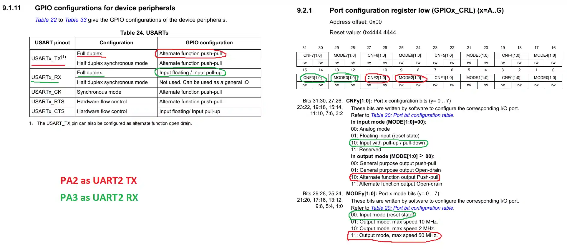
- Here First of all we need to choose the correct mode from the GPIO Configuration for Device Peripherals
- UART TX in full duplex mode should be set as Alternate Function Push Pull
- and UART RX should be set as Input Pull UP
- So we will configure the GPIO Control Register (CRL/CRH) based on this configuration.
GPIOA->CRL = 0;
GPIOA->CRL |= (3<<8);   // output mode 50 MHz for PA2
GPIOA->CRL |= (2<<10);  // Alternate Func Push Pull For PA2

GPIOA->CRL &= ~(3<<12);   // Intput Mode For PA3
GPIOA->CRL |= (2<<14);  // Input Pull Up/ Down For PA3

GPIOA->ODR |= 1<<3; // Pull Up for PA3UART Configuration
Now the Pin Configuration is complete, we will move to the UART Configuration.
The most important Register used in UART configuration is UART Control Register 1 (CR1). Most of the Configuration is done here.
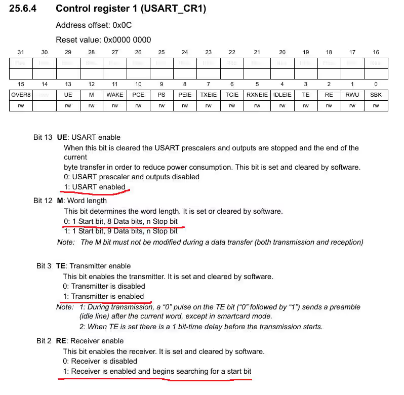
I have only included the important bits in the image. The rest are kept 0 for now. We will modify them as per the requirement in the future.
USART2->CR1 = 0x00;   // Clear ALL
USART2->CR1 |= (1<<13);   // UE = 1... Enable USART
USART2->BRR = (7<<0) | (24<<4);   // Baud rate of 115200, PCLK1 at 45MHz

USART2->CR1 |= (1<<2); // RE=1.. Enable the Receiver
USART2->CR1 |= (1<<3); // TE=1.. Enable Transmitter- We will enable the UART first. To setup other bits, UART needs to be enabled.
- Bit 12 is kept at 0, and it means there will be 1 start bit and 8 Data Bits.
- Then We will enable the Transmitter and Receiver.
- I am also selecting the Baud rate here. The details about the Baud Rate are mentioned below
Selecting the Baud Rate
The Baud Rate can be Programmed into the Baud Rate Register (UART_BRR). The calculation for the Baud Rate is Shown below
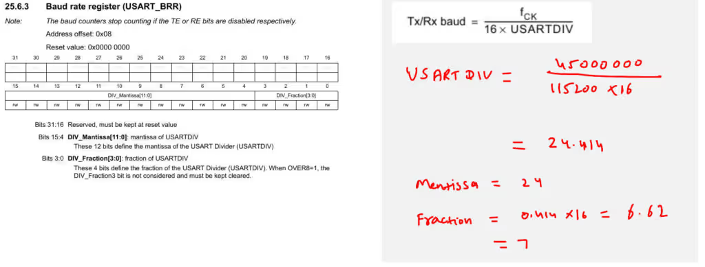
- Here the UART2 is connected to the APB1 Clock, and therefore the Fck = 45 MHz (APB1 Peripheral Frequency)
- Now If we want the Baud Rate of 115200, the MENSTISSA will come equal to 24, and the FRACTION = 7
- We will program these values in the 0th Position (for FRACTION) and in the 4th position (for MENTISSA) in the BRR Register.
This completes the Configuration part of the UART. Now we will see how to send or receive data using the UART
Sending and Receiving Data
To handle the sending and the receiving, the STATUS Register plays a very vital part. Below is the picture of the Status register
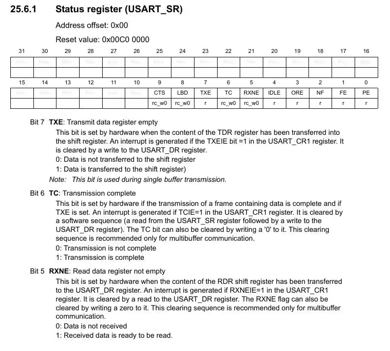
- Here we are mainly interested in these 3 bits.
- TXE bit will be set once the content of the Data Register has been transferred to the Shift Register. Now the Shift Register will start sending the data to the Tx Line.
- In the means time we can put another data byte into the Data Register, and later that byte will also be transferred to the Shift register.
- Once all the data bytes have been transferred (after the stop bit is sent), the TC flag will be set.
- Similarly during the receive, we will wait for the RXNE bit to set.
- This bit is set if there is data in he DATA Register, and once it is confirmed, we can read the data.
void UART2_SendChar (char c)
{
	/*********** STEPS FOLLOWED *************

	1. Write the data to send in the USART_DR register (this clears the TXE bit). Repeat this
		 for each data to be transmitted in case of single buffer.
	2. After writing the last data into the USART_DR register, wait until TC=1. This indicates
		 that the transmission of the last frame is complete. This is required for instance when
		 the USART is disabled or enters the Halt mode to avoid corrupting the last transmission.

	****************************************/

	USART2->DR = c;   // LOad the Data
	while (!(USART2->SR & (1<<6)));  // Wait for TC to SET.. This indicates that the data has been transmitted
}


uint8_t UART2_GetChar (void)
{
		/*********** STEPS FOLLOWED *************

	1. Wait for the RXNE bit to set. It indicates that the data has been received and can be read.
	2. Read the data from USART_DR  Register. This also clears the RXNE bit

	****************************************/
	uint8_t Temp;

	while (!(USART2->SR & (1<<5)));  // Wait for RXNE to SET.. This indicates that the data has been Received
	Temp = USART2->DR;  // Read the data.
	return Temp;
}- Here we will load he data into the Data Register, and wait for the TC bit to set.
- This will indicate that the data has been transferred
- During the receive, we will wait for the RXNE bit to set.
- This will indicate that there is some data available in the Data Register
- Now we will read the data
The Main Function
void delay (uint32_t time)
{
	while (time--);
}

uint8_t buffer[30];
int indx = 0;
int main (void)
{
	SysClockConfig ();
	Uart2Config ();

	while (1)
	{
//		int c = UART2_GetChar ();
//		UART2_SendChar (c);

		UART2_SendString (str);
		delay (100000000);

//		buffer[indx] = UART2_GetChar ();
//		indx++;
//		if (indx>=30) indx = 0;
	}
}Here after initializing the system clock and the UART, we can send or receive data in the while loop.
STM32 Register based Tutorial Series

STM32F103 Clock Setup using Registers
STM32 GPIO Output Example Using Registers | BSRR, MODER, GPIOA Explained
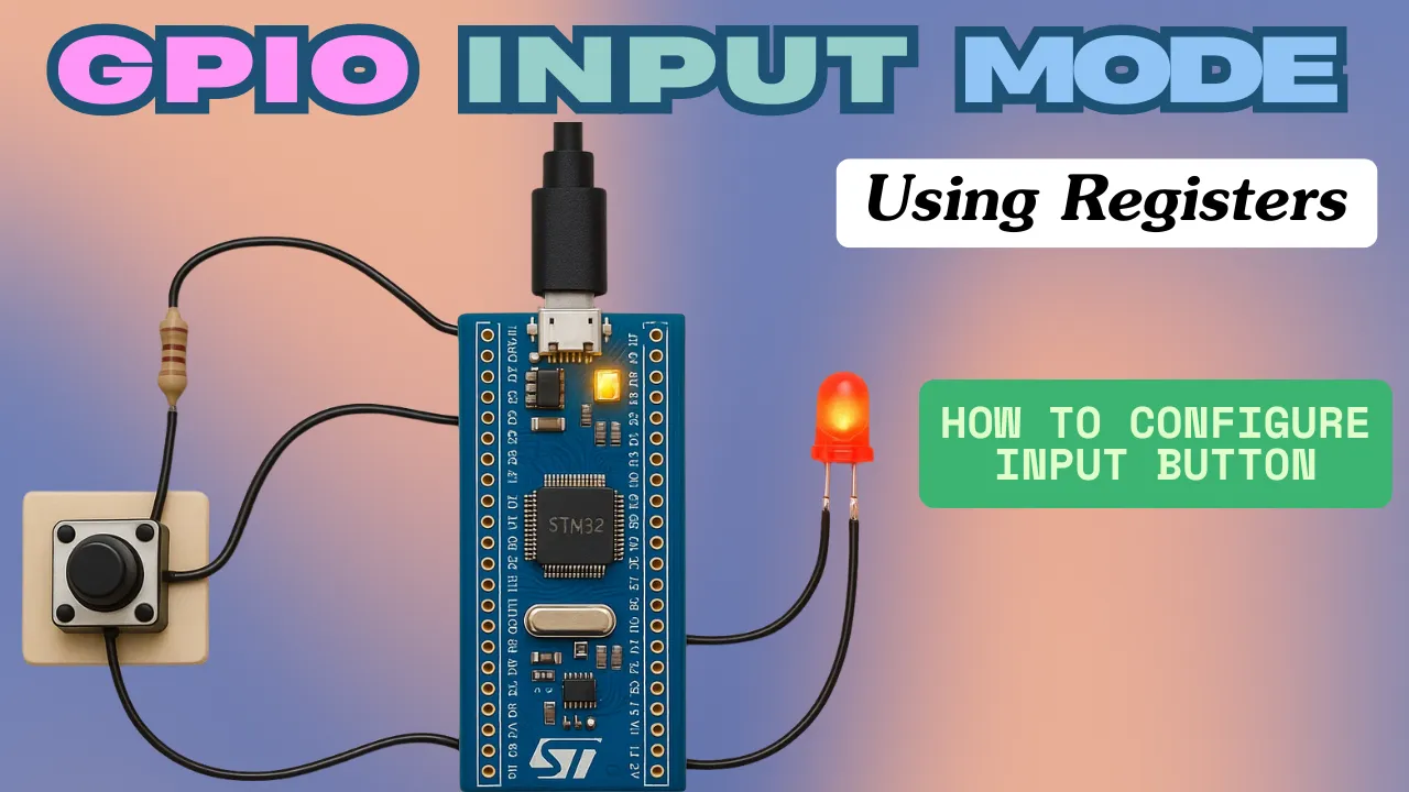
STM32 GPIO Input Configuration – Pin Setup, Pull-Up, and IDR Read
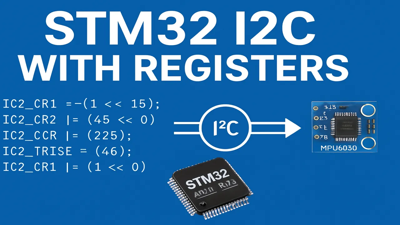
STM32 I2C Tutorial | Register-Based Configuration with Example Code
External Interrupt using Registers
STM32 SPI Tutorial Using Registers (Full-Duplex Master with ADXL345)

DMA with ADC using Registers in STM32


I’m missing how you know which pins are connected to UART2. It’s just stated as a fact that you need PA2 and PA3.
check out the pinout and schematic of your MCU
Install stm32cubemx and if you turn on UART2 then it shows you pins
well explained
i supposed that fort USART_Send_String function you put the Send_char function in for loop according to which size srlen(data) send for example
Yes Exactly.
It’s provided in the final code.
I didn’t feel it’s important to explain here