Last Updated: March 23, 2026
How to interface TM1637 7-segment display with STM32
This is PART1 of the mini tutorial series covering the 7 segment display using TM1637 driver with STM32. In this tutorial series we will everything about this display driver including the method to display the clonk on it.
TM1637 is a kind of LED (light-emitting diode display) drive control special circuit with keyboard scan interface. It is internally integrated with MCU digital interface, data latch, LED high pressure drive and keyboard scan. It is a Two-wire serial interface (CLK, DIO), so the pin requirement is also reduced.
In today’s tutorial we will cover how to connect the display with the STM32, how to configure the cubeMX and how to write the basic functions to display the numbers on it.
VIDEO TUTORIAL
You can check the video to see the complete explanation and working of this project.
Connection
Below is the image showing the connection diagram between the display and the STM32F103C8T6.
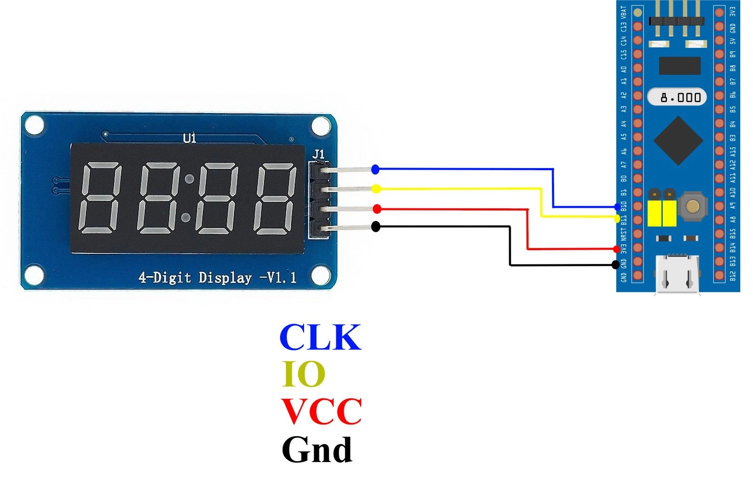
The display I am using is a 4-Digit display with colon (:) in the middle. It is perfect to display the clock data.
The Clock pin of the display is connected to the pin PB10 of the STM32 and the DIO pin is connected to the pin PB11. The display is powered with 3.3V from the MCU itself.
CubeMX Configuration
Let’s take a look at the clock setup first.
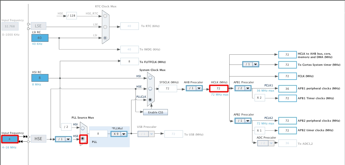
I have configured the external crystal to provide the clock. The Crystal is 8MHz and the system is running at maximum 72MHz.
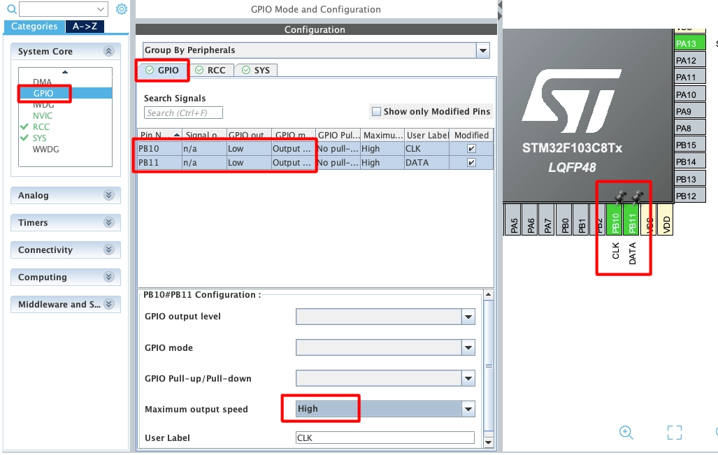
The Pins PB10 and PB11 are configured as output. I have renamed them according to how they are connected to the display.
Go to the GPIO setup and set the maximum output speed of both the pins as HIGH.
This is all the configuration we need to do here.
The Code
As per the datasheet of the device the data must be sent in the following order.
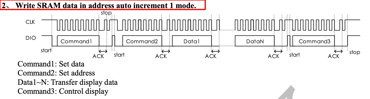
There are mainly 2 ways of writing the data to the display, the Address auto increment mode and the Fixed Address mode. In the auto increment mode one data byte is store at the given address and the next data byte will automatically be stored at the next position. We will use this mode in our tutorial.
Basically we first need to send the command1 (Set Data), then send the command2 (Set Address) followed by the data bytes, and send the command3 (Control Display) at the end.
If you notice the picture carefully, the command1 and command3 are sent between the start and stop. Whereas there is no stop condition between command2 and the data.
Start Condition
As per the reference manual, “When CLK is a high level and DIO changes from high to low level, data input starts“. You can also see the same in the image below.
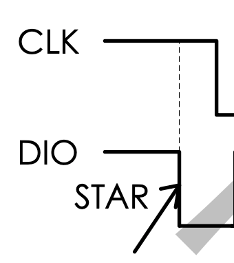
We will write a separate function to generate this start condition.
void start (void)
{
	CLK_HIGH();
	DATA_HIGH();
	Delay_us (2);
	DATA_LOW();
}Here we will first pull the CLK and DATA pins High. Then wait for 2us and pull the DATA pin Low.
This function Delay_us does not actually generates the delay in microseconds. The device datasheet does not specify some particular clock requirement, but it should be fast enoughor else it will not work. Below is the function used for delay purpose.
void Delay_us (int time)
{
	for (int i=0; i<time; i++)
	{
		for (int j=0; j<7; j++)
		{
			__asm__("nop");
		}
	}
}You can also use the same function. Note that the maximum value for the variable j is set to 7 and this is because my system is running at 72 MHz. You can change this value according to your system clock. For eg- If the MCU is running at 100 MHz change it to 10, or if it is running at 50 MHz change it to 5.
You can also experiment with some other value here as the clock requirement is not an issue.
Stop condition
As per the reference manual, “When CLK is a high level and DIO changes from low level to high level, data input ends“. You can also see the same in the image below.
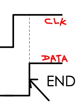
Below is the function to send the stop condition.
void stop (void)
{
	CLK_LOW();
	Delay_us (2);
	DATA_LOW();
	Delay_us (2);
	CLK_HIGH();
	Delay_us (2);
	DATA_HIGH();
}Here we first pull both CLK and DATA to Low. The Pull the CLK high and while it is high, pull the DATA to HIGH.
Write a Byte
Now we will see the function to write a single byte to the device. This byte can be a command or data.
According to the datasheet, “When data is input, DIO signal should not change for high level CLK and DIO signal should change for low level CLK signal.” Basically the data pin should only change while the clock is low.
void writeByte (uint8_t byte)
{
	int i;
	for (i = 0; i<8; i++)
	{
		CLK_LOW();
		if (byte & 0x01) // low front
		{
			DATA_HIGH();
		}
		else
		{
			DATA_LOW();
		}
		Delay_us (3);
		byte = byte >> 1;
		CLK_HIGH();
		Delay_us (3);
	}
}- Here we will first pull the CLK to Low.
- Then check the Least Significant bit of the data byte.
- If the bit is a 1, pull the data pill High or else pull the Data pin Low.
- Then shift the data byte to the right by 1 place and pull the CLK pin High.
This way the data bit is only transferred while the clock is low. We repeat this process for the entire byte.
Check for the ACK
The device sends the Acknowledgement for every byte it receives, whether it’s a command byte or the data byte. Below is the image showing the Acknowledgement bit.
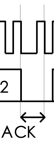
As you can see in the image above, first the CLK needs to be pulled Low. The delay after pulling the CLK low is comparatively higher than the rest of the CLK signal.
At this point, the Data pin should be checked. If the Data pin is LOW, the device has ACKed the data.
Then the CLK is pulled back to High, wait for some time and Pull it Back to Low.
void waitforAck (void)
{
	CLK_LOW();
	Delay_us (5); // After the falling edge of the eighth clock delay 5us
	              // ACK signals the beginning of judgment
//	while (dio);  // Check the state of the Data pin
	CLK_HIGH();
	Delay_us (2);
	CLK_LOW();
}- Here we Pull the CLK Low and then wait for 5us. This delay is larger than the usual clock cycle.
- Since the Data pin is set as output, we can’t check its state, so I am skipping the step here. Assuming if the data has been sent correctly, the Data pin must be Low.
- The pull the CLK pin High, give the usual Delay for the clock cycle and Pull the CLK pin Low again.
Write Data
Finally we will now write a function to send the data to the display. Below is the image showing the pattern to write the data.
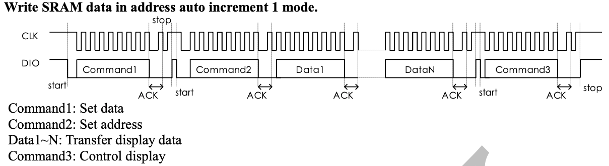
In order to write the data to the display, we need to send the command1 (Set Data), then send the command2 (Set Address) followed by the data bytes, and send the command3 (Control Display) at the end.
If you notice the picture carefully, the command1 and command3 are sent between the start and stop conditions. Whereas there is no stop condition between command2 and the data.
Set Data Command
Below is the table shown for the Set Data command.
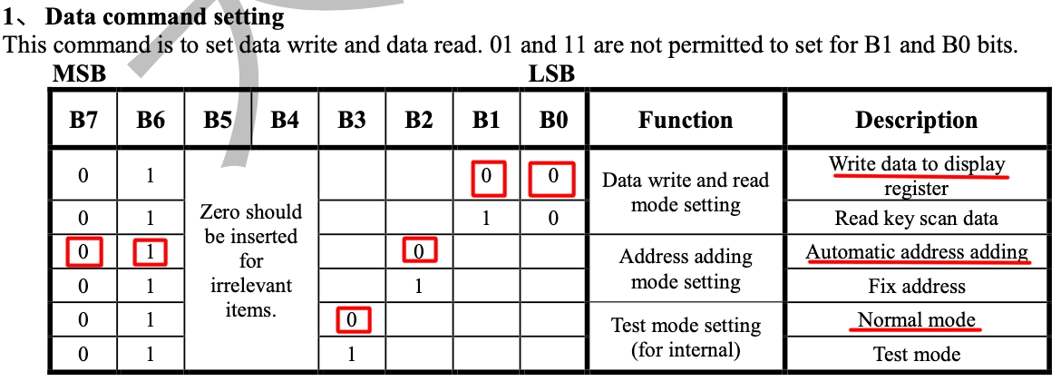
We want to write the data to the display in the Automatic Address Normal Mode. The command Byte will be 0x40.
void TM1637_WriteData (uint8_t Addr, uint8_t *data, int size)
{
	start();
	writeByte(0x40);
	waitforAck();
stop();The TM1637_WriteData function will be used for sending the data to the display. The function takes the following parameters:
- @Addr is the Display address where you want to print the data.
- @data is the pointer to the data array
- @size is the size of the data array.
Command1 (Set Data) should be sent between the start and stop conditions. Also we need to wait for the ACK signal after writing a byte to the device.
Set Address Command
Below is the table shown for the Set Address command.
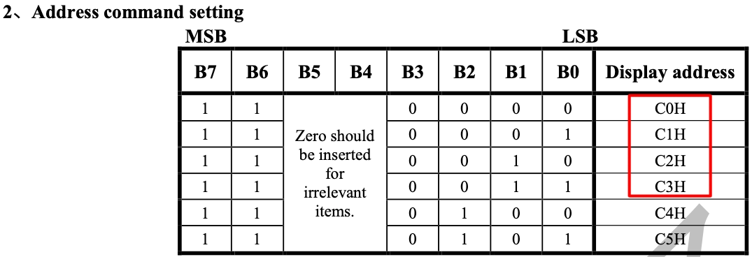
The Address command is used to set the address of the Display. Since we have a 4 digit display, the command can vary between 0xC0 – 0xC3. Below is the image showing the Address for each digit.
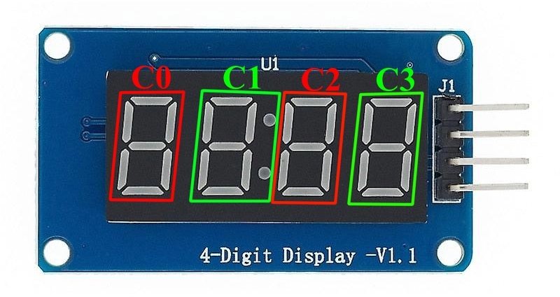
Note that the colon (:) in the middle is a part of the address 0xC1. This colon is controlled by the Most Significant bit of the data sent to the address 0xC1.
	start();
	writeByte(Addr);
	waitforAck();
	for (int i=0; i<size; i++)
	{
		writeByte(data[i]);
		waitforAck();
	}
stop();After sending the Address command, we will continue to send the data to the display. Since we are using the Auto Address increment mode, the new Data will be displayed at the new Address.
After all the data has been sent to the display, issue the Stop condition.
Display Control Command
Below is the table shown for the Display Control command.
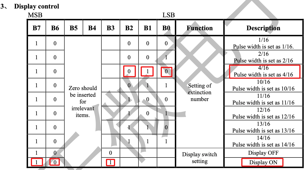
The display control command is used to turn the display On/Off. It is also used to set the display brightness. The brightness is controlled by the PWM, so the higher the duty cycle the brighter the display is.
I am setting the brightness to 4/16 and the display will obviously be turned on. This makes the display control command value as 0x8A.
	start();
	writeByte(0x8A);
	waitforAck();
	stop();
}The Main file
Each digit of the display has 7 segments, i.e 7 Lights. Each segment can be controlled by an individual bit. Below is the image showing the segments.
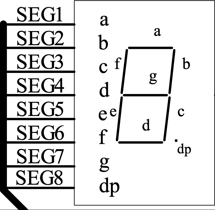
As you can see in the image above, the 7 segments are marked from a to g. As I mentioned each segment is controlled by an individual bit.
The data byte consists of these segments as 0bxgfedcba. Here x represents that the bit is irrelevant and rest of the letters represents the corresponding segments.
Let’s assume I want to display the number 1. To do so, I need to turn on the segments b and c. The binary data for the number 1 will be 0b00000110.
Similarly, If I want to display the number 2, I need to turn on the segments a, b, g, e and d. The binary data for the number 2 will be 0b01011011.
Keeping this in mind we will write the main function.
int main ()
{
  .....
  .....
  uint8_t data[4] = {0b00000110, 0b01011011, 0b01001111, 0b01100110};  // 1, 2, 3, 4
  TM1637_WriteData(0xC0, data, 4);
  while (1)
  { }
}Here we will first store the data for the numbers 1 to 4 in an array.
Then call the WriteData function to send the 4 bytes array to the address 0xC0. Since the address is going to auto increment, we will see each number printed on individual digit of the display.
Result
Below is the image showing the output of the above code.
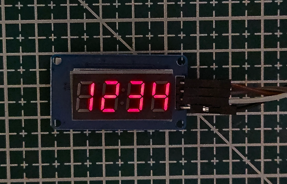
You can see we have the numbers 1 2 3 4 being displayed on individual digits.
