Home ▸ STM32 Tutorials ▸ ADC Series ▸
Updated On: April 16, 2026
STM32 ADC External Trigger Source Selection using Timers
In most basic ADC setups, conversions are started by software, but this approach relies on the CPU, which means timing can vary slightly due to interrupts or code execution delays. In this tutorial, we replace software triggering with a hardware timer, so the ADC starts sampling at a fixed, precise interval every time regardless of what the CPU is doing. This technique is essential for real-time applications like motor control, signal processing, and synchronized multi-channel measurements where consistent timing is critical.
We will configure the ADC to use a timer’s update event as the external trigger source, covering the full setup for STM32F103, STM32F446, and STM32H750. We will also walk through the timer prescaler and ARR calculations needed to achieve the target sampling rate, combine DMA in circular mode for continuous data capture, and handle the Cortex-M7 specific MPU setup for cache coherency.
This is the 7th tutorial in the STM32 ADC series. You can go through the other parts of this series, here are the links:
- STM32 ADC Conversion Time & Frequency Explained
- ADC Injected Conversion Mode
- STM32 ADC Hardware Oversampling
- ADC Reference Voltage Explained
- ADC in Differential Mode
Table Of Contents
- Why Use a Hardware Trigger for STM32 ADC Instead of Software?
- STM32 ADC External Trigger: How It Works (Timing Diagram)
- STM32F103 ADC External Trigger Setup: TIM3 & DMA Config
- STM32F446 ADC External Trigger Setup: TIM2 & DMA Config
- STM32H750 ADC External Trigger Setup: TIM1 & DMA Config
- Wiring Diagram: Connect Potentiometers to STM32 ADC
- STM32 ADC External Trigger: HAL Code & DMA Setup
- STM32 ADC External Trigger Output: Debugger & Logic Analyzer
- STM32 ADC External Trigger with Timers — Video Tutorial
- Download STM32 ADC External Trigger Project Files
- STM32 ADC External Trigger — Frequently Asked Questions
Why Use a Hardware Trigger for STM32 ADC Instead of Software?
In most STM32 ADC tutorials, conversions are often started by software. While this works for simple applications, it has limitations in terms of timing precision and CPU load. Using an external trigger — typically generated by a hardware timer, PWM, or another peripheral — allows the ADC to start sampling and converting automatically at precise, consistent intervals. This is especially important in real-time applications, such as motor control, sensor fusion, or signal processing, where consistent timing and synchronization are critical.
External triggers ensure that ADC conversions are not affected by software delays, interrupt routines, or varying CPU load. When combined with DMA, this approach allows high-speed, continuous data acquisition without occupying the processor, freeing it for other tasks.
For Precise and Consistent Sampling Intervals
Software-triggered conversions depend on the CPU executing instructions, which may vary slightly due to interrupts, background tasks, or code execution delays. In contrast, hardware-triggered ADCs use a dedicated timer or peripheral signal, ensuring that each conversion starts exactly at the programmed interval. This guarantees uniform sampling, which is critical for applications like waveform analysis, audio data capture, or any measurement requiring accurate timing.
To Synchronize ADC with Other Peripherals
When ADC sampling needs to be coordinated with other peripherals, such as PWM outputs for motor control or timer events in a control loop, an external trigger ensures perfect synchronization. For example, you can configure a timer to generate a trigger signal at the exact moment a PWM pulse occurs, ensuring that the ADC captures the signal at a consistent point in the cycle.
To Reduce CPU Overhead
With software-triggered ADC, the CPU must explicitly start each conversion. This adds overhead and may limit the maximum achievable sampling rate. Using an external trigger in combination with DMA in circular mode offloads the CPU completely: conversions and data transfers occur automatically, allowing the processor to focus on other critical tasks.
To Improve Multi-Channel ADC Timing
When scanning multiple ADC channels in sequence, external triggers ensure that each set of channel conversions starts at the same instant every cycle. This guarantees consistent timing across channels and reduces timing jitter, which is essential for synchronized sensor readings or real-time signal processing.
The table below summarises the differences between Software Start and External trigger source.
| Feature | Software Start | External Trigger |
|---|---|---|
| Timing Precision | Varies depending on CPU execution and interrupts | Fixed and precise, controlled by hardware (timers or peripherals) |
| CPU Load | High, CPU must start each conversion | Low, CPU can remain free during conversions |
| Synchronization with Peripherals | Difficult to achieve | Easy, perfect alignment with timers, PWM, or external events |
| Multi-Channel Consistency | May vary if software delays occur | Consistent timing for all channels |
| Use Case | Simple testing, occasional ADC reads | Real-time control, waveform sampling, multi-channel synchronized measurements |
STM32 ADC External Trigger: How It Works (Timing Diagram)
Below is an image illustrating the sequence of events when using an external trigger with the STM32 ADC:
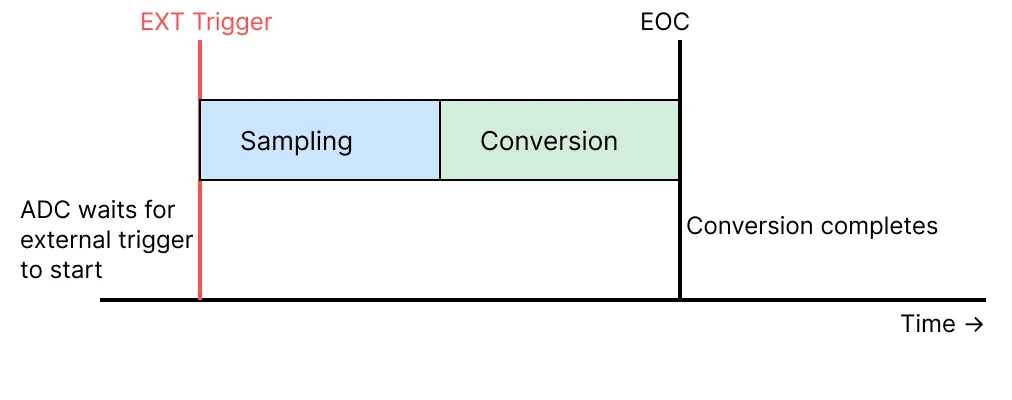
- EXT Trigger: A timer or external event triggers the ADC conversion.
- Sampling: The ADC samples the input signal.
- Conversion: The sampled signal is converted to a digital value.
- EOC (End of Conversion): Data becomes available, optionally transferred via DMA.
STM32F103 ADC External Trigger Setup: TIM3 & DMA Config
In this section, we will configure the STM32F103C8 ADC using CubeMX. You’ll learn how to select ADC channels, set sampling times, configure external triggers, and enable DMA or continuous conversion modes.
ADC Configuration
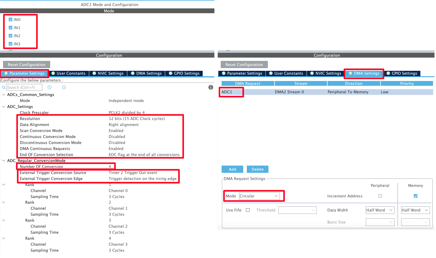
Below is the image showing the ADC configuration for multiple channels.
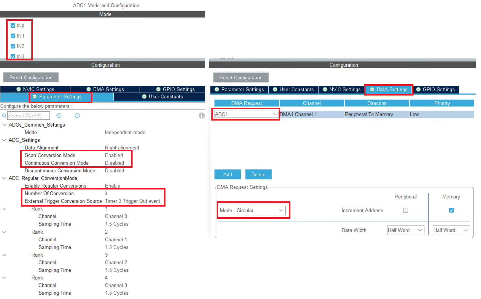
I have enabled 4 channels of the ADC1. This is where the 4 potentiometers will be connected to.
Since we are using 4 different Channels of ADC1, set the Number of Conversions (under ADC_Regular_ConversionMode) to 4. This will automatically enable the Scan Conversion Mode, which is necessary in case of Multiple Channels.
You can configure the Rank and Sampling Time for each channel. The Rank determines the sequence in which the channels will be converted.
The Continuous Conversion Mode should be Disabled. Doing so will make sure the ADC does not start another conversion for all the channels automatically. Instead we will use the timer’s event to start the conversion. This way we can control the sampling rate of the ADC channels.
The External Trigger Conversion Source is set to Timer3 Trigger out Event. So whenever the Timer3 will generate an event, it will start the conversion in the ADC1.
In the DMA section, add the DMA request for the ADC1. Also make sure that the DMA is configured in the Circular Mode. In this mode the DMA will transfer the data continuously.
The F103C8 has 12 bit ADC resolution by default and we don’t have the option to configure it. Therefore the data width for the DMA must be set to Half-Word (16 bits).
Timer Configuration
We will use Timer3’s event to trigger the ADC conversion. Before we configure the timer, we must find more details about where this timer is connected to. Below is the image showing some details about it.
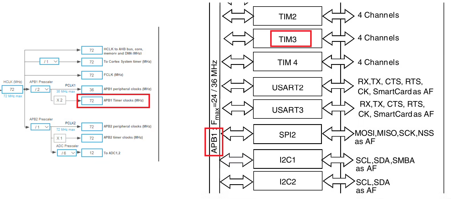
The second half of the image above is taken from the F103C8 Datasheet. It shows that the TIM3 is connected to the APB1 Bus. The first Half of the image is showing the clock configuration for this project. The APB1 Timer clock is running at 72MHz clock, so this will be the TIM3 clock as well.
We will now configure the TIM3’s Prescaler and ARR to reduce this clock to the desired ADC sampling rate we need.
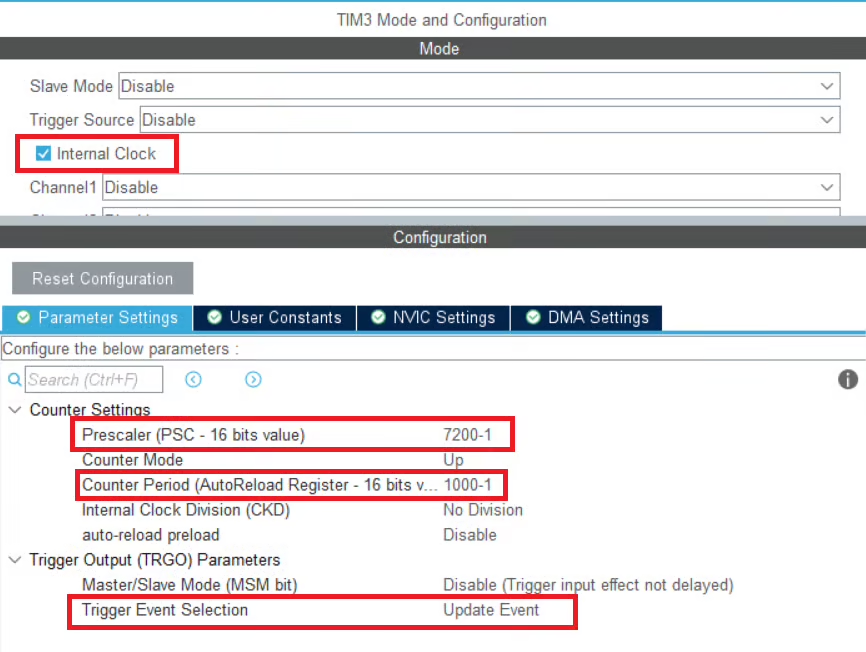
We will first use the internal clock as the clock source for TIM3, which is running at 72 MHz. To generate a suitable trigger for the ADC, we configure the prescaler and auto-reload register (ARR) as follows.
Step 1: Apply the Prescaler
The prescaler divides the timer clock:
After the prescaler, the timer counts at 10 kHz.
Step 2: Apply the Auto-Reload Register (ARR)
The ARR determines how many timer ticks occur before an update event (overflow) is generated:
This means the timer will generate an update event every 0.1 s, which we can use to trigger the ADC conversion.
Step 3: Select the Trigger Event
In CubeMX, choose “Update Event” in the ADC Trigger Event selection. This configures the ADC to start a conversion each time the TIM3 counter overflows.
How it Works
- Using this method ensures precise, hardware-controlled ADC sampling at 10 Hz.
- TIM3 counter starts from 0 and counts up.
- When the counter reaches the ARR value, it overflows.
- This overflow generates an update event, which is then used as the external trigger for the ADC.
STM32F446 ADC External Trigger Setup: TIM2 & DMA Config
Similar to the STM32F103C8 configuration, here we will see how to configure the STM32F446RE. We will start with the ADC configuration first.
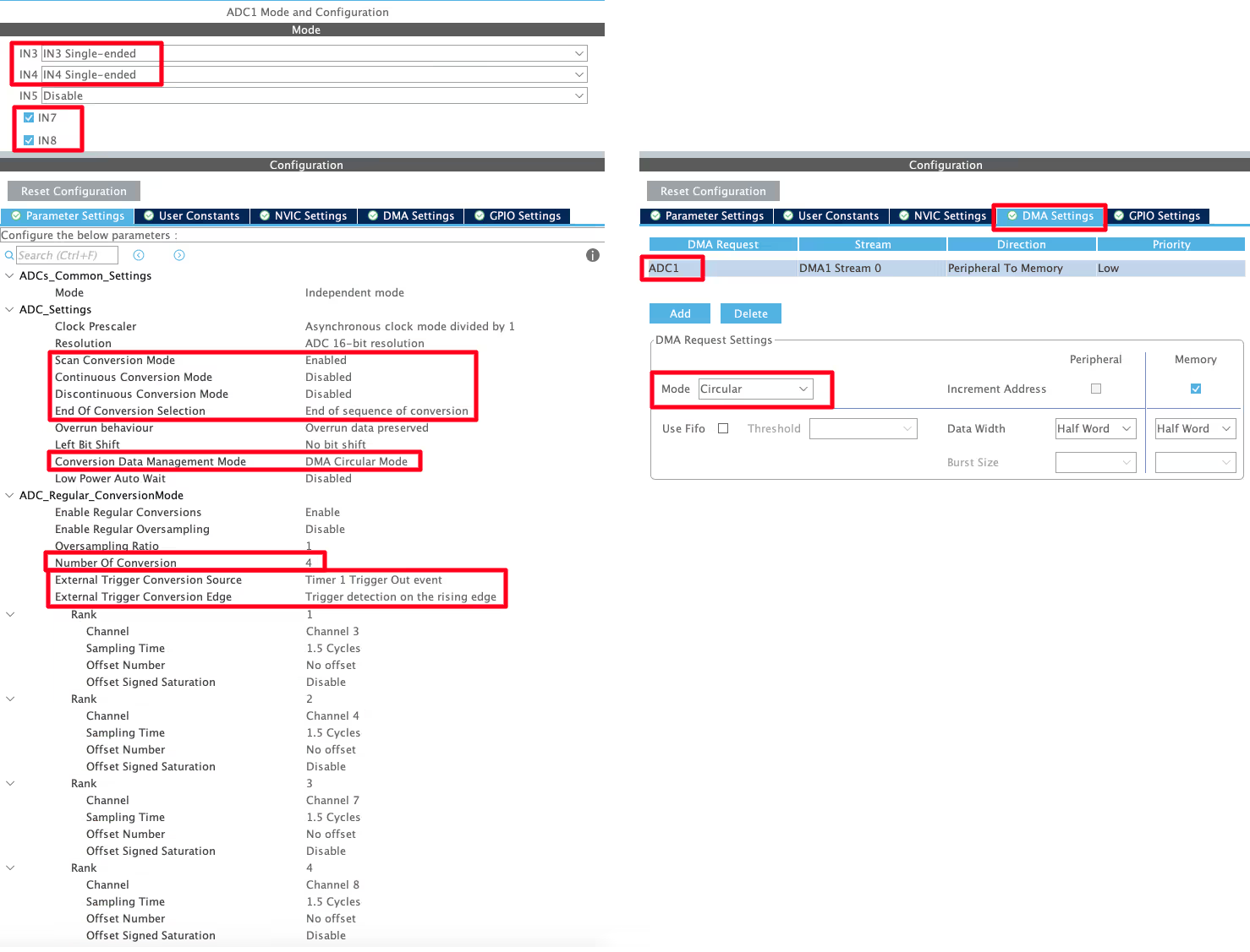
ADC Configuration
Below is the image showing the ADC configuration for multiple channels.
I have enabled 4 channels of the ADC1. This is where the 4 potentiometers will be connected to.
Since we are using 4 different Channels of ADC1, set the Number of Conversions (under ADC_Regular_ConversionMode) to 4. This will automatically enable the Scan Conversion Mode, which is necessary in case of Multiple Channels.
You can configure the Rank and Sampling Time for each channel. The Rank determines the sequence in which the channels will be converted.
The Continuous Conversion Mode should be Disabled. Doing so will make sure the ADC does not start another conversion for all the channels automatically. Instead we will use the timer’s event to start the conversion. This way we can control the sampling rate of the ADC channels.
The External Trigger Conversion Source is set to Timer2 Trigger out Event. So whenever the Timer2 will generate an event, it will start the conversion in the ADC1.
The DMA Continuous Request must also be Enabled. This is to make sure that the DMA requests the data continuously from the ADC. This mode should be kept Enabled while using the DMA in Circular mode.
The End of Conversion Selection should be set at the end of all the conversions. Doing this will make sure that the Conversion complete interrupt in only triggered when all the 4 channels (one complete sequence) have been converted.
In the DMA section, add the DMA request for the ADC1. Also make sure that the DMA is configured in the Circular Mode. In this mode the DMA will transfer the data continuously. Set the data width as per the ADC Resolution. I have configured the ADC with 12bits resolution, therefore the data width is set to half word (16bits).
Timer Configuration
We are using Timer2’s event to trigger the ADC conversion. Before we configure the timer, we must find more details about where this timer is connected to. Below is the image showing some details about it.
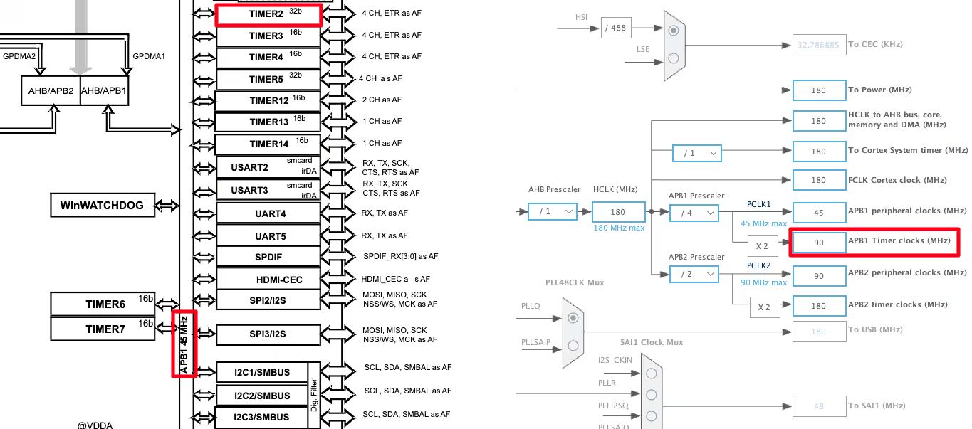
The First half of the image above is taken from the F446RE Datasheet. It shows that the TIM2 is connected to the APB1 Bus. The Second Half of the image is showing the clock configuration for this project. The APB1 Timer clock is running at 90MHz clock, so this will be the TIM2 clock as well.
We will now configure the TIM2’s Prescaler and ARR to reduce this clock to the desired ADC sampling rate we need.
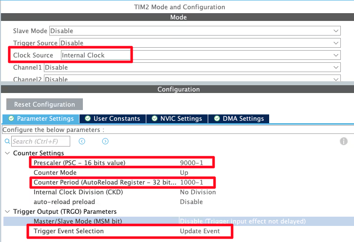
We will first enable the internal clock as the clock source for TIM2, which is running at 90 MHz. To generate a trigger suitable for the ADC, we configure the prescaler and auto-reload register (ARR) as follows.
Step 1: Apply the Prescaler
The prescaler divides the timer clock to slow it down:
After applying the prescaler, TIM2 counts at 10 kHz.
Step 2: Apply the Auto-Reload Register (ARR)
The ARR determines how many timer ticks occur before an update event (overflow) is generated:
This means TIM2 will generate an update event every 0.1 s, which will serve as the ADC trigger.
Step 3: Configure ADC Trigger Event
In CubeMX, select “Update Event” as the ADC trigger source. This ensures that each time TIM2 overflows, it triggers an ADC conversion automatically.
How It Works
- TIM2 counter starts at 0 and increments with each tick of the prescaled clock.
- When the counter reaches the ARR value (1000), it overflows.
- The overflow generates an update event, which is then used by the ADC as an external trigger.
- This setup ensures precise, hardware-timed ADC sampling at 10 Hz without CPU intervention.
STM32H750 ADC External Trigger Setup: TIM1 & DMA Config
Let’s configure the STM32H750 Microcontroller now. We will again start with the ADC configuration first.
ADC Configuration
Below is the image showing the ADC configuration for multiple channels.
I have enabled 4 channels of the ADC1. This is where the 4 potentiometers will be connected to.
Since we are using 4 different Channels of ADC1, set the Number of Conversions (under ADC_Regular_ConversionMode) to 4. This will automatically enable the Scan Conversion Mode, which is necessary in case of Multiple Channels.
You can configure the Rank and Sampling Time for each channel. The Rank determines the sequence in which the channels will be converted.
The Continuous Conversion Mode should be Disabled. Doing so will make sure the ADC does not start another conversion for all the channels automatically. Instead we will use the timer’s event to start the conversion. This way we can control the sampling rate of the ADC channels.
The External Trigger Conversion Source is set to Timer1 Trigger out Event. So whenever the Timer1 will generate an event, it will start the conversion in the ADC1.
The Conversion Data Management Mode should be set to DMA Circular. This is to make sure that the DMA does requests the data continuously from the ADC. This mode should be used while using the DMA in Circular mode.
The End of Conversion Selection should be set at the end of sequence of conversion. Doing this will make sure that the Conversion complete interrupt in only triggered when all the 4 channels (one complete sequence) have been converted.
In the DMA section, add the DMA request for the ADC1. Also make sure that the DMA is configured in the Circular Mode. In this mode the DMA will transfer the data continuously. I have configured the ADC resolution of 16bits, therefore the data width is set to Half-Word (16bits).
Timer Configuration
We are using Timer2’s event to trigger the ADC conversion. Before we configure the timer, we must find more details about where this timer is connected to. Below is the image showing some details about it.
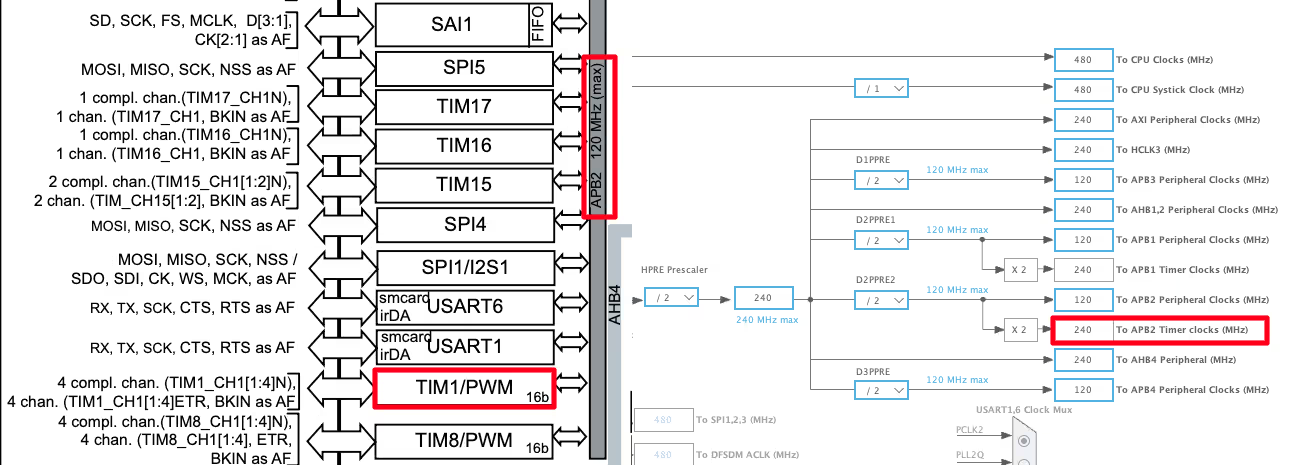
The First half of the image above is taken from the H750 Datasheet. It shows that the TIM1 is connected to the APB2 Bus. The Second Half of the image is showing the clock configuration for this project. The APB2 Timer clock is running at 240MHz clock, so this will be the TIM1 clock as well.
We will now configure the TIM1’s Prescaler and ARR to reduce this clock to the desired ADC sampling rate we need.
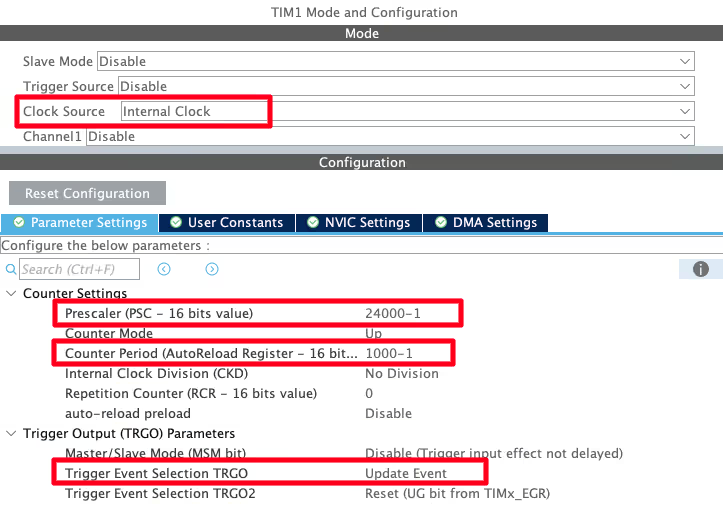
We will first enable the internal clock as the clock source for TIM1, which is running at 240 MHz. To generate a trigger suitable for the ADC, we configure the prescaler and auto-reload register (ARR) as follows.
Step 1: Apply the Prescaler
The prescaler reduces the timer clock to a lower frequency:
After applying the prescaler, TIM1 counts at 10 kHz.
Step 2: Apply the Auto-Reload Register (ARR)
The ARR determines how many timer ticks occur before an update event (overflow) is generated:
This means TIM1 will generate an update event every 0.1 s, which will serve as the ADC trigger.
Step 3: Configure ADC Trigger Event
In CubeMX, select “Update Event” as the ADC trigger source. This ensures that each time TIM1 overflows, it triggers an ADC conversion automatically.
How It Works
- TIM1 counter starts at 0 and increments with each tick of the prescaled clock.
- When the counter reaches the ARR value (1000), it overflows.
- The overflow generates an update event, which is used by the ADC as an external trigger.
- This setup ensures precise, hardware-timed ADC sampling at 10 Hz without CPU intervention.
Cortex M7 Related Changes
In this section we will cover the configuration and code exclusively needed for the cortex M7 devices.
We know that as per ST’s recommendation, we should use the Instruction and Data cache to improve the system performance. But if the cache are enabled, the DMA will always have the cache coherency issue. This is why we will use the Memory Processing Unit (MPU) of the cortex M7 to deal with the cache coherency.
Below is the image showing the MPU configuration in the cortex M7 Devices.
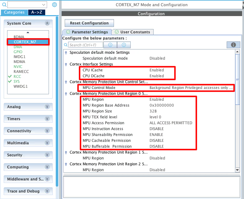
As you can see in the image above, I have enabled both Instruction and Data Cache (ICache & DCache).
We also need to enable the MPU in the MPU_PRIVILEGED_DEFAULT mode. Here I am choosing the Base Address region 0x30000000, this is the region for the RAM_D2 and we will relocate our buffer in this region.
- Here I have selected the 32 Bytes region, since it’s the least size available. The ADC Buffer is going to be 20 bytes in size.
- The rest of the configuration is to set the region as non-cacheable region. This would prevent the cache coherency issue between the CPU and the DMA.
In the main file, we need to relocate the ADC_VAL array to the RAM_D2 Region, 0x30000000. We can do this by using the section attribute as shown below.
__attribute__((section(".adcarray"))) uint16_t ADC_VAL[4];Here I am relocating the ADC_VAL array to the section “.adcarray“. The section (.adcarray) will be defined in the flash script file as shown below.
  .mysection (NOLOAD):
  {
    . = ABSOLUTE(0x30000000);
    *(.adcarray)
} >RAM_D2As you can see above, the section (.adcarray) is linked to the region RAM_D2 (0x30000000).
The rest of the code remains the same as we used in the DMA section.
Wiring Diagram: Connect Potentiometers to STM32 ADC
Below is the image showing the connection between the potentiometers and the H750.
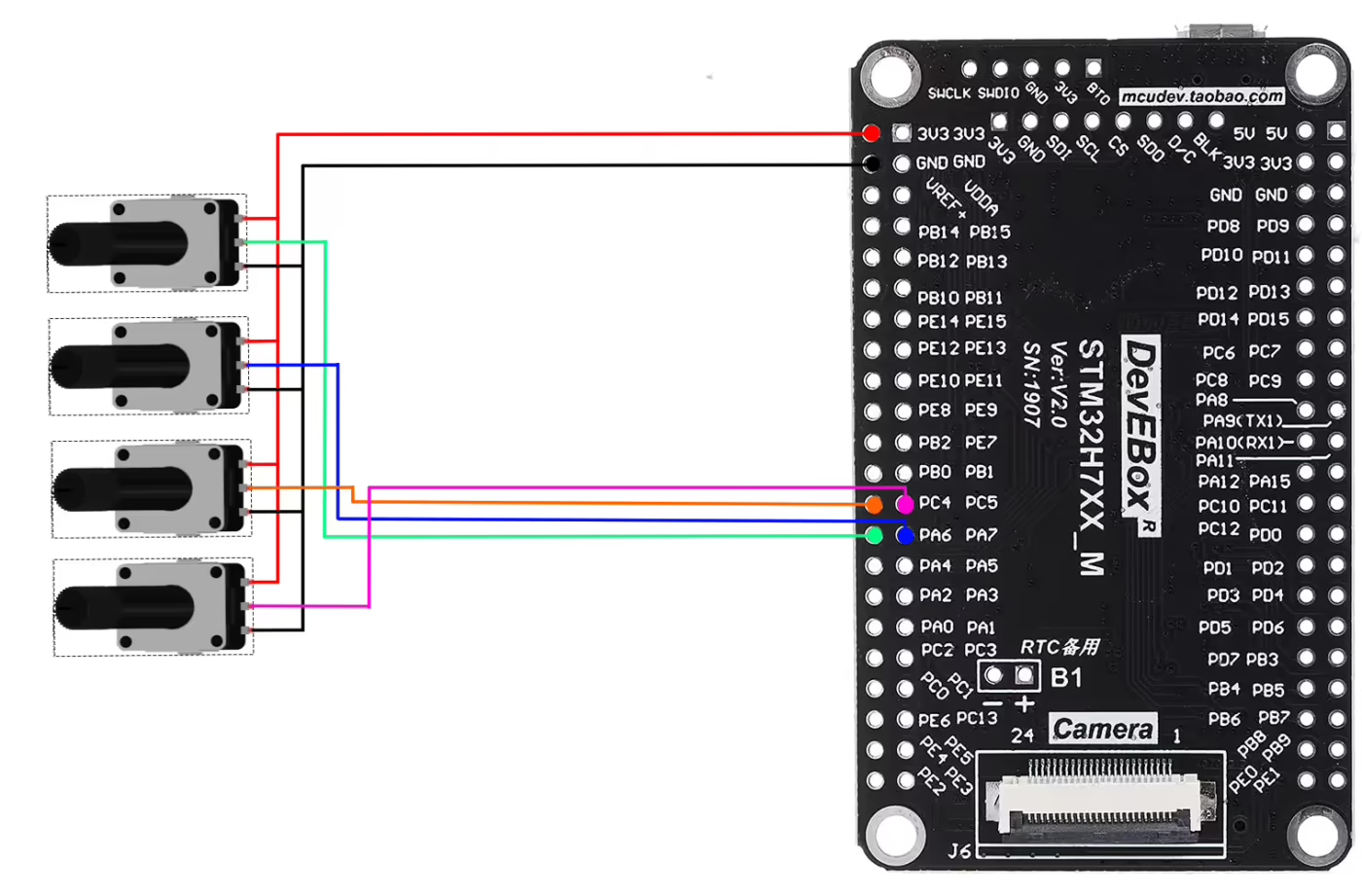
As shown in the image above, four potentiometers are connected to four input pins of the MCU, each corresponding to a separate ADC channel. These pins allow the ADC to read the analog voltage from each potentiometer independently.
The potentiometers are powered from the MCU’s 3.3 V supply, and their wipers provide a variable voltage to the ADC inputs, ranging from 0 V to 3.3 V. This setup allows us to measure and monitor the voltage level of each potentiometer in real time, demonstrating multi-channel ADC operation on the STM32 microcontroller.
STM32 ADC External Trigger: HAL Code & DMA Setup
The code will remain the same for all the STM32 MCUs. If there are any changes, I will specify in this section itself.
Definitions
Let’s define some variables, which we will use in the main function later.
//uint16_t ADC_VAL[4];
__attribute__((section(".adcarray"))) uint16_t ADC_VAL[4]; // cortex M7 onlyADC_VAL is an array of 4 elements of 16 bit in size. We will use this array to store the converted ADC Value. Even if you are using 10bits, 12bits or 14bits resolution the ADC_VAL will still be defined as a 16 bit variable.
The main function
Below is the main function.
int main()
{
  ....
  HAL_TIM_Base_Start(&htim1);
  HAL_ADC_Start_DMA(&hadc1, ADC_VAL, 4);
  while (1)
  {
  }
}Inside the main function we will first start the TIM1 in the base mode. This will start will Timer’s counter, which will start counting up. Once the counter overflows, an event will trigger, which will start the ADC conversions. The counter than resets back to 0 and starts counting UP again.
Next we will start the ADC in DMA Mode.The parameter ADC_VAL is the array where we want to store the converted data, and 4 is the number of conversions we want the DMA to transfer.
Once the ADC finishes all the conversions, an interrupt will trigger and the ADC Conversion Callback will be called.
void HAL_ADC_ConvCpltCallback(ADC_HandleTypeDef *hadc)
{
  HAL_GPIO_TogglePin(GPIOA, GPIO_PIN_1);
}Inside this callback we will toggle the pin PA1. This pin toggles each time the callback is called and hence it can be used to calculate the time interval of the callback function. We will measure it on the scope.
STM32 ADC External Trigger Output: Debugger & Logic Analyzer
Below is the gif showing the ADC channel data on the debugger.
As you can see above, the ADC data is updating every 100ms. This is because we have set the Timer’s output to 10Hz. To confirm if this is indeed 100ms, we can view the toggling time of the pin PA1 on the logic analyzer. Below is the image showing the same.
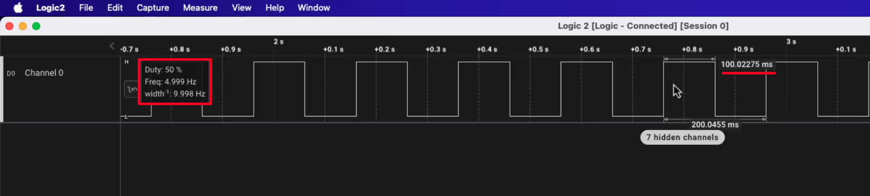
As you can see above, the pin PA1 remains HIGH and LOW for 100ms. This means that the pin Toggles every 100ms. This is because the Conversion Complete Callback is called every 100ms. Which signifies that the ADC sampling frequency is set to 10Hz.
STM32 ADC External Trigger with Timers — Video Tutorial
Watch the complete walkthrough of this tutorial — configuring ADC external trigger sources in CubeMX for STM32F103, F446, and H750, calculating timer prescaler and ARR values for a 10Hz sampling rate, enabling DMA circular mode, and verifying the 100ms trigger interval on a logic analyzer.
Download STM32 ADC External Trigger Project Files
Complete CubeMX projects for STM32F103, STM32F446, and STM32H750, covering timer-triggered ADC with DMA circular mode and Cortex-M7 MPU configuration. Free to download — support the work if it helped you.
STM32 ADC External Trigger — Frequently Asked Questions
Conclusion
In this tutorial, we covered how to configure STM32 ADC to start conversions using a hardware timer as an external trigger source. We walked through the full CubeMX setup for the F103, F446, and H750 — selecting the correct timer, calculating the prescaler and ARR values for a 10Hz sampling rate, enabling DMA in circular mode for continuous data transfer, and handling the Cortex-M7 MPU configuration to prevent cache coherency issues. The trigger timing was then verified on a logic analyzer by measuring the toggle interval of a GPIO pin toggled inside the conversion complete callback.
Using a hardware timer as an ADC trigger removes all timing uncertainty from software-based approaches. The CPU never touches the conversion process — the timer fires, the ADC samples, and the DMA transfers the result, all automatically at the programmed interval. This makes the technique ideal for any application where consistent, predictable sampling is required, such as waveform capture, sensor fusion, or synchronized multi-channel readings.
In the next tutorial, we will look at ADC injected conversion mode, where high-priority ADC channels can interrupt an ongoing regular conversion sequence to capture time-critical measurements on demand. If you found this tutorial useful, stay tuned for that one.
Browse More STM32 ADC Tutorials
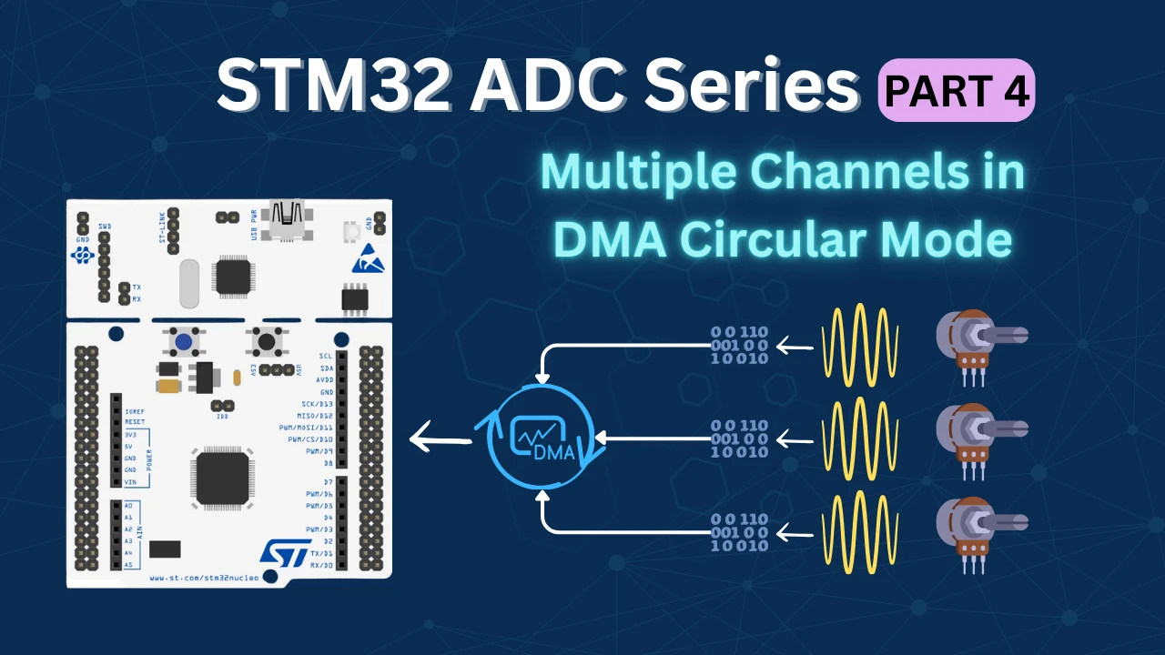
STM32 ADC Multiple Channels with Circular DMA: CubeMX Setup & HAL Code
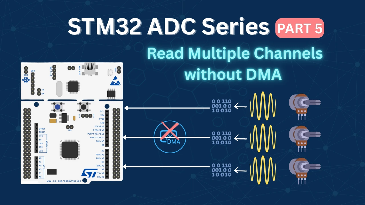
STM32 ADC Multiple Channels Without DMA: CubeMX Setup & HAL Code
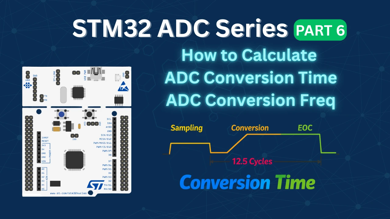
STM32 ADC Conversion Time: Formula, Calculation & Frequency Explained
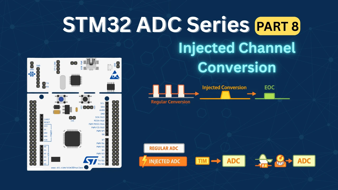
STM32 ADC Injected Conversion Mode: Triggered & Auto Injection
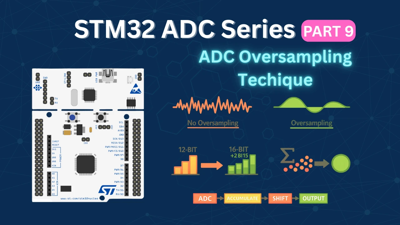
STM32 ADC Hardware Oversampling: Improve Resolution & Reduce Noise
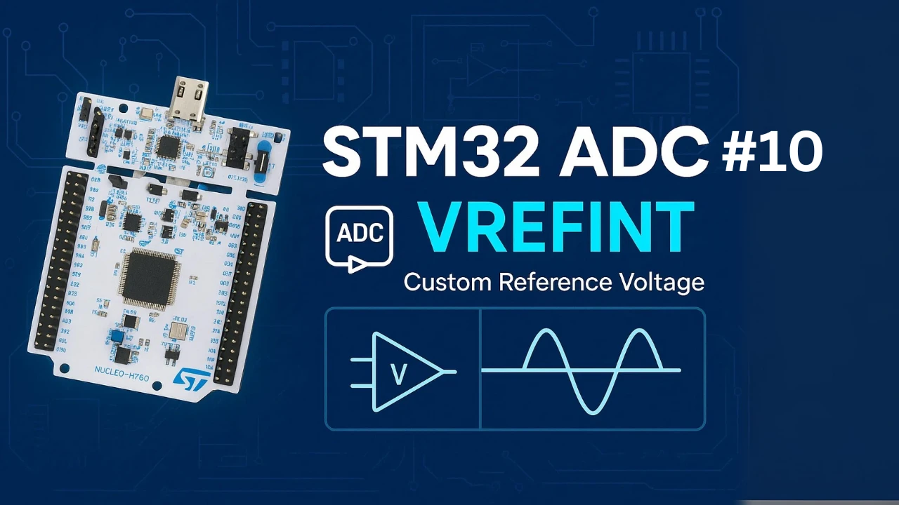
STM32 ADC Reference Voltage: VREFINT, VREF+ & VREFBUF
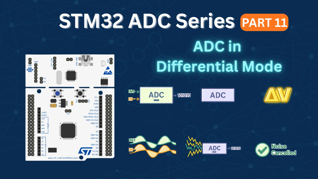
STM32 ADC Differential Mode: Setup, CMV, and HAL Code Guide


Download button downloads PART4 not PART7
Thanks for informing. It has been fixed now.