Home ▸ STM32 Tutorials ▸ ADC Series ▸
Updated On: April 16, 2026
STM32 ADC Differential Mode: Measuring Voltage Between Two Inputs
In this tutorial, we’ll explore how to use the ADC differential mode on STM32 microcontrollers to measure the voltage difference between two analog inputs instead of a single-ended signal relative to ground. Differential mode is especially useful for applications requiring noise rejection, precise small-signal measurement, and bidirectional sensing. You’ll learn how to bias the inputs, respect the ADC’s common-mode voltage requirements, configure the differential inputs in STM32CubeMX, and convert the raw ADC result into a meaningful differential voltage reading.
This is the 11th tutorial in the STM32 ADC series. You can go through the other parts of this series, here are the links:
- STM32 ADC Conversion Time & Frequency Explained
- ADC External Trigger Source Selection
- ADC Injected Conversion Mode
- STM32 ADC Hardware Oversampling
- ADC Reference Voltage Explained
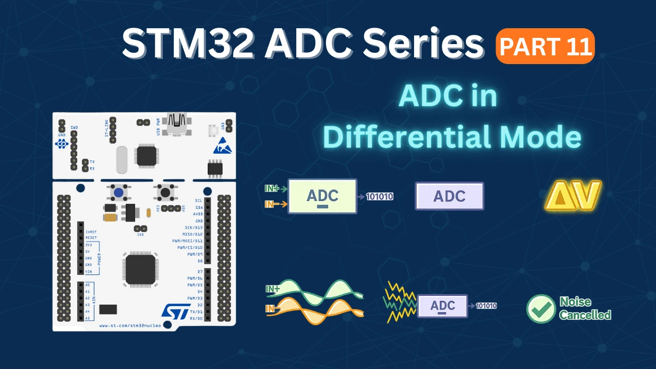
Table Of Contents
- How STM32 ADC Differential Mode Works: Biasing and CMV Requirements
- When to Use STM32 ADC Differential Mode: Key Use Cases
- STM32 ADC Differential Mode CubeMX Setup: INP and INN Pin Config
- STM32 ADC Differential Mode: Wiring Diagram
- STM32 Differential ADC: HAL Code and Voltage Conversion Formula
- STM32 ADC Differential Mode Output: CMV Range Verified
- STM32 ADC Differential Mode — Video Tutorial
- Download STM32 ADC Differential Mode Project Files
- STM32 ADC Differential Mode — Frequently Asked Questions
How STM32 ADC Differential Mode Works: Biasing and CMV Requirements
Differential ADCs are generally used in applications requiring high precision, noise reduction, and increased dynamic range. In this tutorial we will specifically focus on just measuring the voltage difference between the two differential inputs. The ADC data will be based on this differential voltage, which we will later convert into the voltage.
Not all the STM32 devices support differential ADC. I am going to use the STM32H7 based custom development board.
As mentioned in the reference manual both the differential inputs should be biased at Vref/2. The Vref is a custom reference voltage which can be provided externally, but the hardware on the board should be configured accordingly. By default the Vref is connected to the VDDA (& VCC), therefore the Vref is 3.3V.
Biasing means that instead of fluctuating around 0V, the signals should be centred around 1.65V.
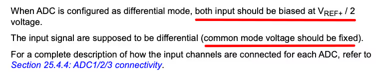
We should also take care of the Common mode voltage (CMV). This Common-mode voltage is the average voltage of two input signals in a differential system. This voltage only has a small range in STM32. You can see it in the image from datasheet of the device.
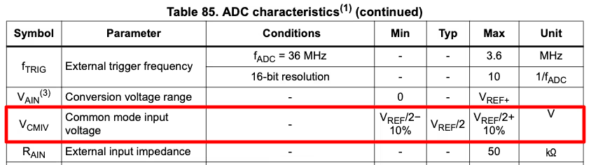
You can see the common mode voltage varies by only 10% from Vref/2 voltage. So if the Vref is at 3.3V, the common mode voltage can vary from around 1.48 V to 1.82V.
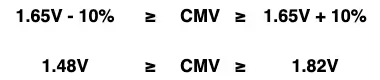
When choosing the input voltages on both the differential pairs make sure the average of both voltages lies within this range. It does not mean that it will not work outside this range rather the result outside this range is unpredictable. In certain cases it might work while in other cases it won’t.
The ADC will convert the voltage difference between both the input pins as per the formula shown below.
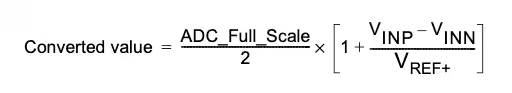
- If the VINN = 0 and VINP = VREF, the ADC value will be equal to the MAXIMUM.
- Whereas when VINN = VREF and VINP = 0, the ADC value will be equal to the 0.
- When VINN = VINP, the ADC value will be exactly HALF the MAXIMUM.
Below is the image showing the range of ADC value based on the differential inputs. The VDIFF is the voltage difference between the input signals.
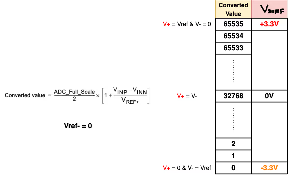
We will write our code in such a way that the ADC MAXIMUM (65535) indicates a +3.3V while the ADC MINIMUM (0) indicates a -3.3V. Also the ADC MAX/2 (32768) will indicate 0V.
When to Use STM32 ADC Differential Mode: Key Use Cases
In many real-world applications, measuring a signal with respect to ground is not enough. Signals often ride on top of noise, ground offsets, or common-mode voltages that can significantly affect the accuracy of single-ended ADC measurements. Differential ADC mode solves this problem by measuring the voltage difference between two input pins, effectively rejecting noise that is common to both signals.
One of the biggest advantages of differential mode is noise immunity. Any interference picked up equally on both input lines—such as switching noise, EMI, or ground fluctuations—is largely canceled out during conversion. This makes differential ADC ideal for environments with motors, switching regulators, or long sensor cables where noise is unavoidable.
Differential mode is also extremely useful when working with low-level or bipolar signals. Sensors such as current shunts, strain gauges, pressure sensors, and certain audio or industrial sensors often produce very small voltage differences that can be easily lost in noise when measured single-ended. By directly measuring the difference between the two inputs, the ADC can capture these small changes more accurately.
Another important use case is when the signal is not referenced to ground. In such cases, forcing a single-ended measurement can lead to incorrect readings or even violate ADC input limits. Differential ADC mode allows the signal to float within a valid common-mode range while still providing a correct measurement of the voltage difference.
STM32 ADC Differential Mode CubeMX Setup: INP and INN Pin Config
Before moving to the code, let’s quickly look at the STM32CubeMX configuration. In this case, there isn’t much to configure manually, most of the work is simply enabling the ADC and selecting the required channel in differential mode.
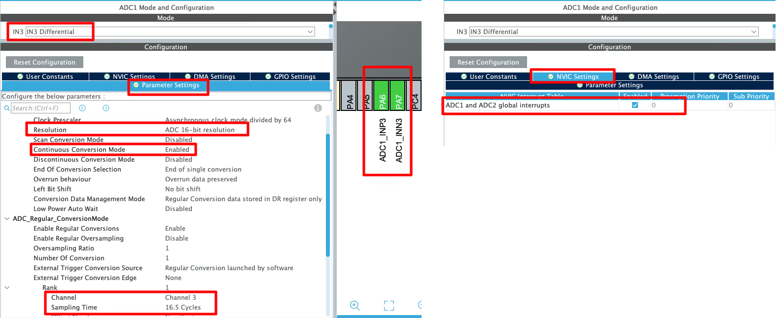
ADC Channel 3 is configured to operate in differential mode. In this configuration, pin PA6 is selected as the INP (positive) input, while pin PA7 is assigned as the INN (negative) input. The ADC conversion result therefore represents the voltage difference between PA6 and PA7, rather than the voltage of a single pin with respect to ground.
The ADC is set to continuous conversion mode, which allows a new conversion to start automatically as soon as the previous one completes. This ensures a steady stream of differential measurements without requiring software to restart each conversion manually. Additionally, the ADC interrupt is enabled so that the CPU is notified immediately when a conversion is complete, making it easier to process or log the converted data in real time.
STM32 ADC Differential Mode: Wiring Diagram
The Connection for this project is shown in the image below.
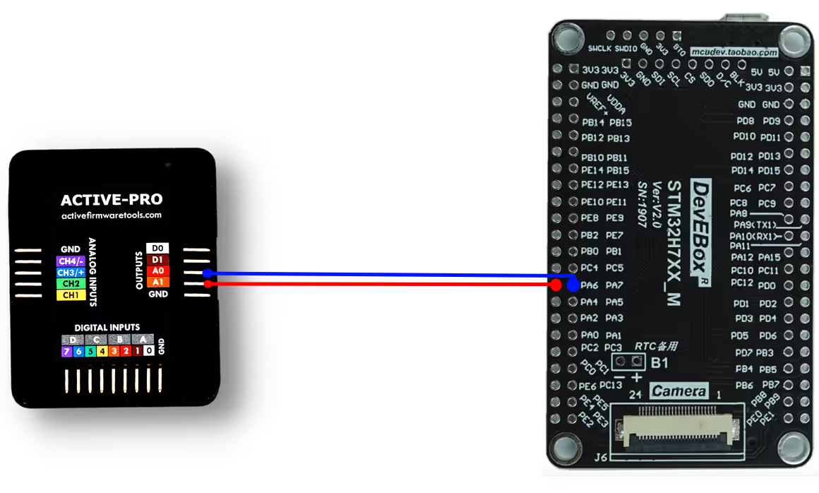
I am using Active Pro Debugger to provide variable voltages to the ADC input. The A1 pin is connected to the PA6 (+ve Input) whereas the A0 pin is connected to the PA7 (-ve Input).
STM32 Differential ADC: HAL Code and Voltage Conversion Formula
uint16_t ADC_VAL;
int voltage;The variable ADC_VAL will be used to store the Raw ADC value. This value is generated by the ADC based on the difference in voltage between the inputs. The variable voltage will store the voltage data based on the Raw value.
Inside the main function we will start the ADC in interrupt mode. Once the conversion is finished, an interrupt will trigger and the ConvCpltCallback will be called. Inside this callback we will simply set the variable isDone. The data will be processed in the while loop.
int isDone =0;
void HAL_ADC_ConvCpltCallback(ADC_HandleTypeDef *hadc)
{
	isDone = 1;
}Below is the main function.
int main ()
{
  ....
  ....
  HAL_ADC_Start_IT(&hadc1);
  while (1)
  {
    if (isDone)
    {
	  ADC_VAL = HAL_ADC_GetValue(&hadc1);
	  voltage = (3300*2*ADC_VAL/65535)-3300;
	  isDone = 0;
    }
    HAL_Delay(250);
  }
} Inside the while loop we will check if the variable isDone is set. If it is, we will read the Raw ADC value.
Then convert this Raw value to the voltage. By default the Vref is connected to VDDA (&VCC), therefore the Vref = 3.3V. Hence the value 3300 is used here. We want to convert the RAW ADC value to the voltage ranging from +Vref to -Vref, hence this formula is used baed on the examples provided by ST.
STM32 ADC Differential Mode Output: CMV Range Verified
Below are the images showing the output of the above code. When the +ve Input is at 0V and -ve Input is at 3.3V, the average input voltage is 1.5V, which is within the Common Mode Voltage (CMV ) range. The Raw ADC value is near 0 and the converted voltage (Difference between INP and INN) is -3.3V.
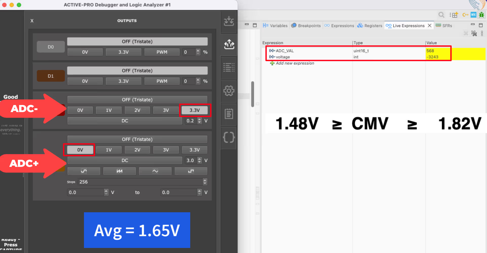
When the +ve Input is at 3.3V and -ve Input is at 0V, the average input voltage is 1.5V, which is within the Common Mode Voltage (CMV ) range. The Raw ADC value is 65535 and the converted voltage (Difference between INP and INN) is 3.3V.
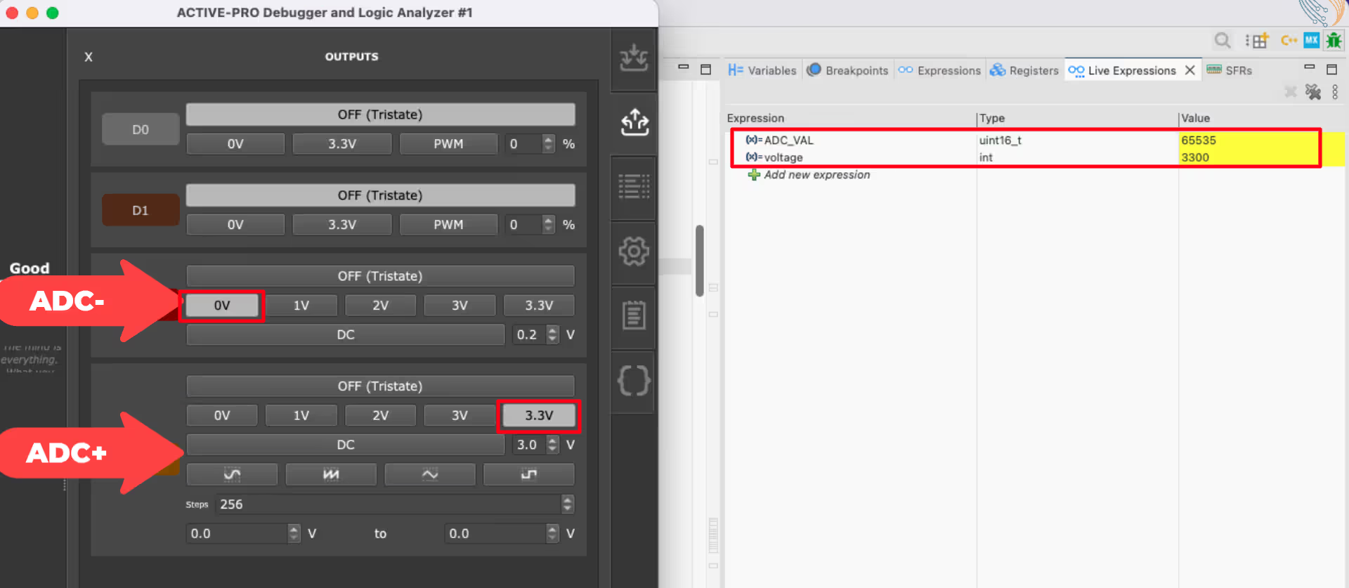
When both the +ve Input and -ve Input are equal at 1.6V, the average input voltage is 1.6V, which is within the Common Mode Voltage (CMV ) range. The Raw ADC value is near Half the MAX and the converted voltage (Difference between INP and INN) is 0V.
When the +ve Input is at 3V and -ve Input is at 1V, the average input voltage is 2.5V, which is far outside the Common Mode Voltage (CMV) range. The ADC behaviour is unpredictable at this point. You can see in the image below the converted voltage is wrong.
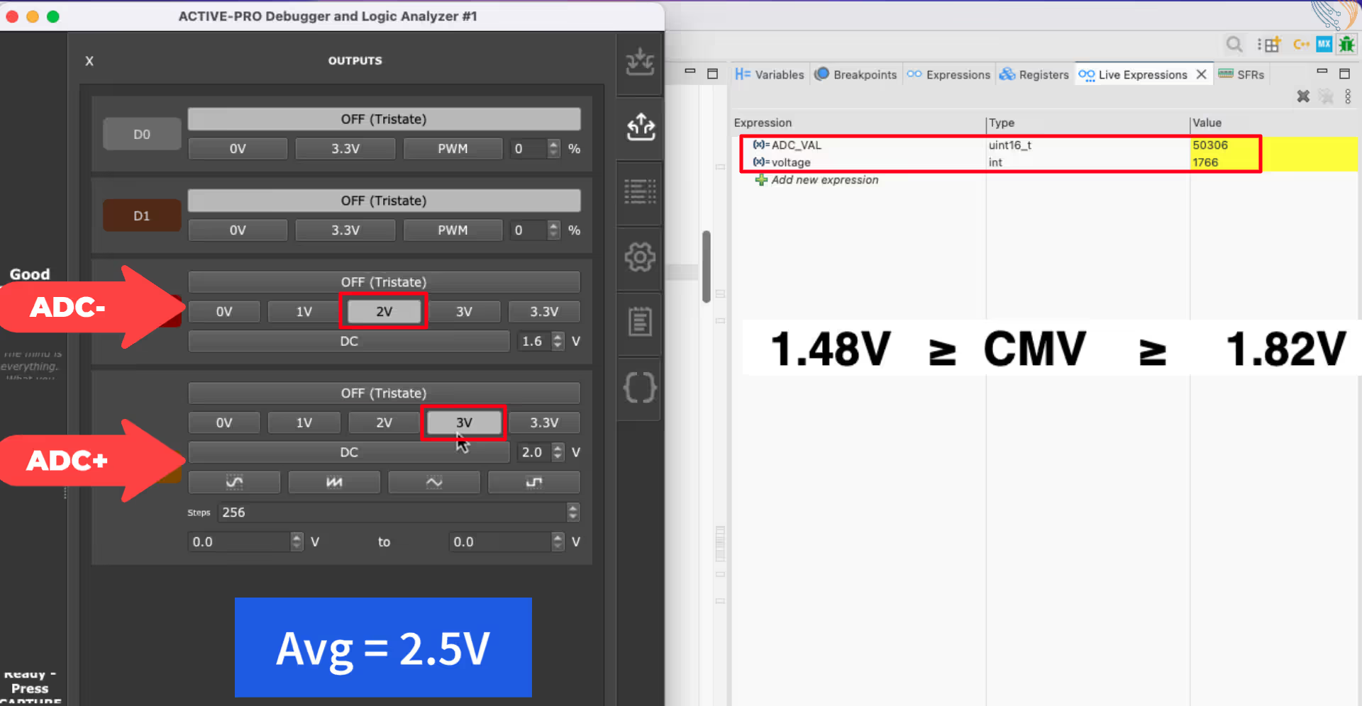
Hence while designing the differential ADC, we must take care that the average input voltage of the two inputs must lie within the CMV range.
STM32 ADC Differential Mode — Video Tutorial
Watch the complete walkthrough of this tutorial — understanding differential inputs, biasing requirements, and common-mode voltage limits, configuring the INP and INN pins in CubeMX, writing the HAL code to convert raw ADC values into a signed differential voltage, and testing the output across multiple input conditions.
Download STM32 ADC Differential Mode Project Files
Complete CubeMX project for the STM32H750, including differential ADC configuration, interrupt-based HAL code, and signed voltage conversion formula. Free to download — support the work if it helped you.
STM32 ADC Differential Mode — Frequently Asked Questions
Conclusion
In this tutorial, we covered how to configure and use STM32 ADC differential mode to measure the voltage difference between two analog inputs. We explained the biasing requirement, the common-mode voltage range and why exceeding it produces unreliable results, and how to configure a differential input pair in CubeMX on the STM32H7. We then wrote the HAL code to convert the raw 16-bit ADC result into a meaningful signed voltage reading spanning from −3.3V to +3.3V, and verified the output across several input conditions in the debugger.
Differential ADC mode is the right choice whenever your signal is not referenced to ground, when noise immunity is important, or when you need to measure small voltage differences accurately. The common-mode voltage constraint is the most important thing to get right — keep the average of both inputs within roughly 10% of Vref/2, and the ADC will behave predictably. Violate it, and the results become unreliable regardless of how clean your signal is.
Browse More STM32 ADC Tutorials
STM32 ADC Multiple Channels with Circular DMA: CubeMX Setup & HAL Code
STM32 ADC Multiple Channels Without DMA: CubeMX Setup & HAL Code
STM32 ADC Conversion Time: Formula, Calculation & Frequency Explained
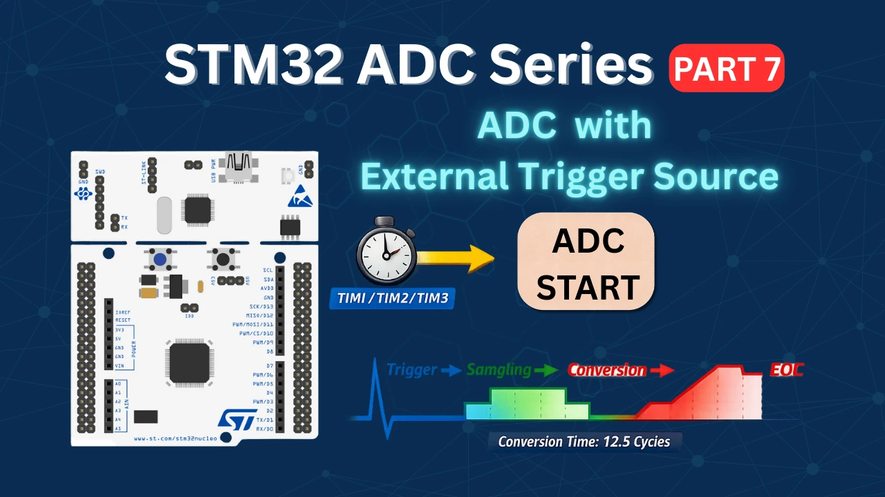
STM32 ADC External Trigger with Timer: CubeMX & HAL Guide
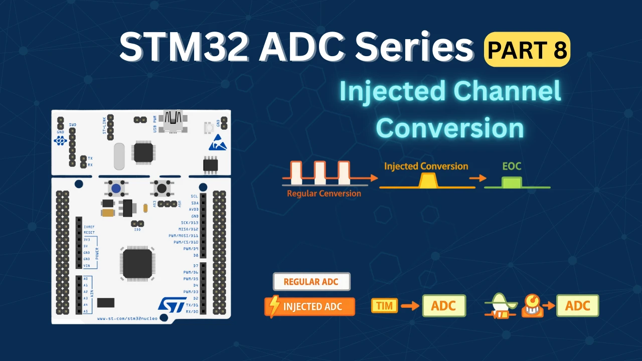
STM32 ADC Injected Conversion Mode: Triggered & Auto Injection
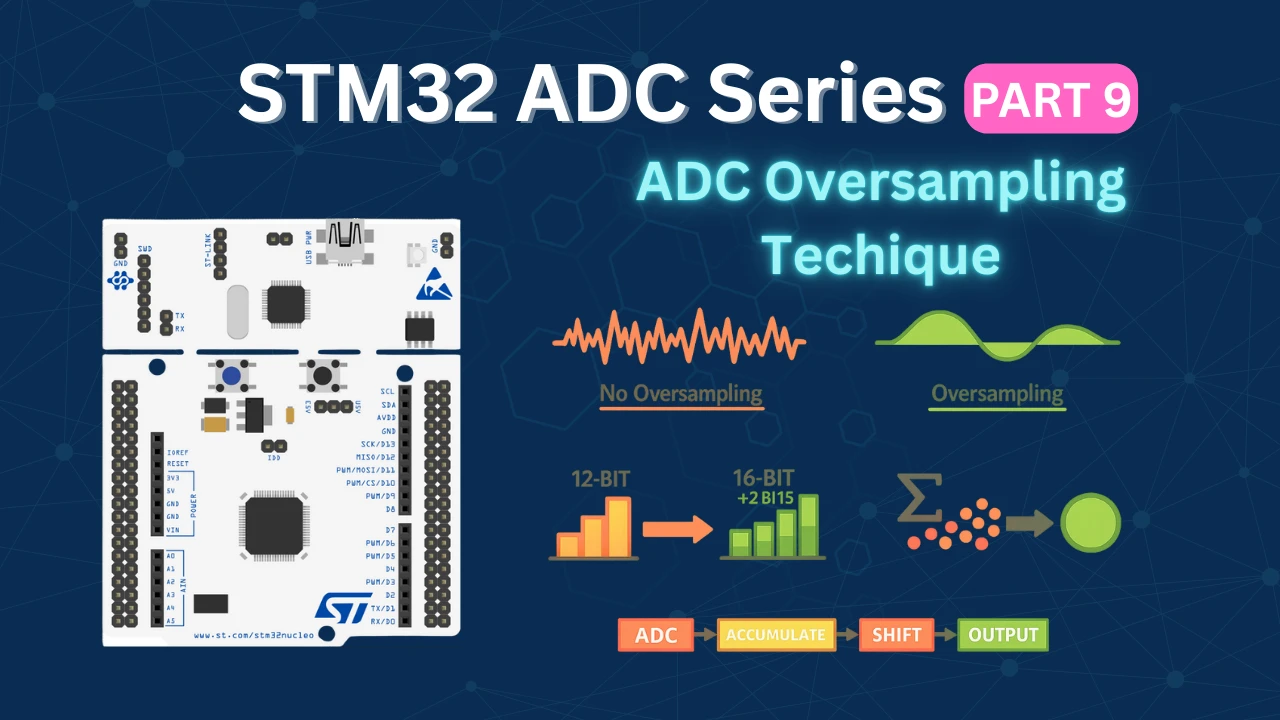
STM32 ADC Hardware Oversampling: Improve Resolution & Reduce Noise
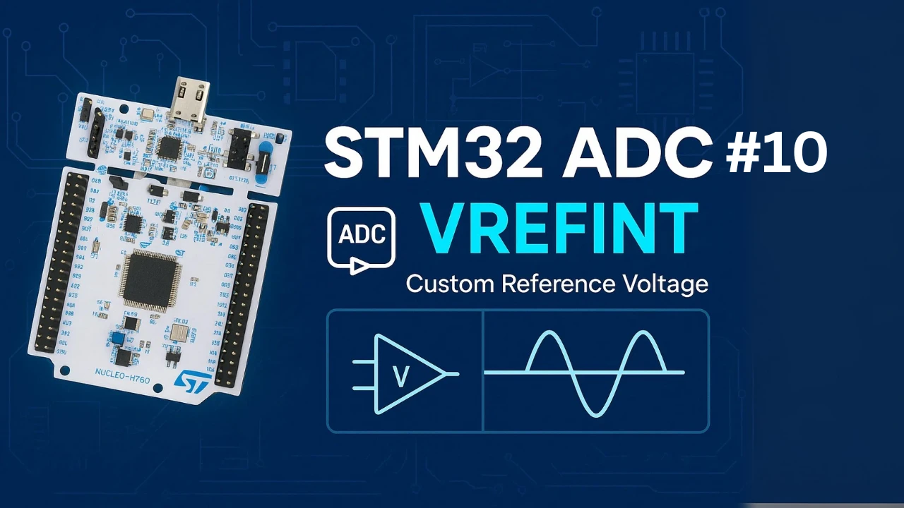
STM32 ADC Reference Voltage: VREFINT, VREF+ & VREFBUF


Hi, can we use DACA