
Home ▸ STM32 Tutorials ▸ ADC Series ▸
Updated On: April 16, 2026
STM32 ADC Hardware Oversampling: How to Improve Resolution and Reduce Noise
ADC oversampling is a powerful technique that allows STM32 microcontrollers to extract more useful information from analog signals without adding extra hardware. By intelligently combining multiple ADC samples, oversampling can significantly reduce noise and improve the effective resolution of measurements.
In this tutorial, we explore how ADC oversampling works in STM32 MCUs, how it is implemented using CubeMX, and what impact it has on conversion time and sampling rate. With practical configuration steps and real output observations, you’ll see when oversampling makes sense and how to use it correctly in your applications.
This is the 9th tutorial in the STM32 ADC series. You can go through the other parts of this series, here are the links:
- STM32 ADC Conversion Time & Frequency Explained
- ADC External Trigger Source Selection
- ADC Injected Conversion Mode
- ADC Reference Voltage Explained
- ADC in Differential Mode
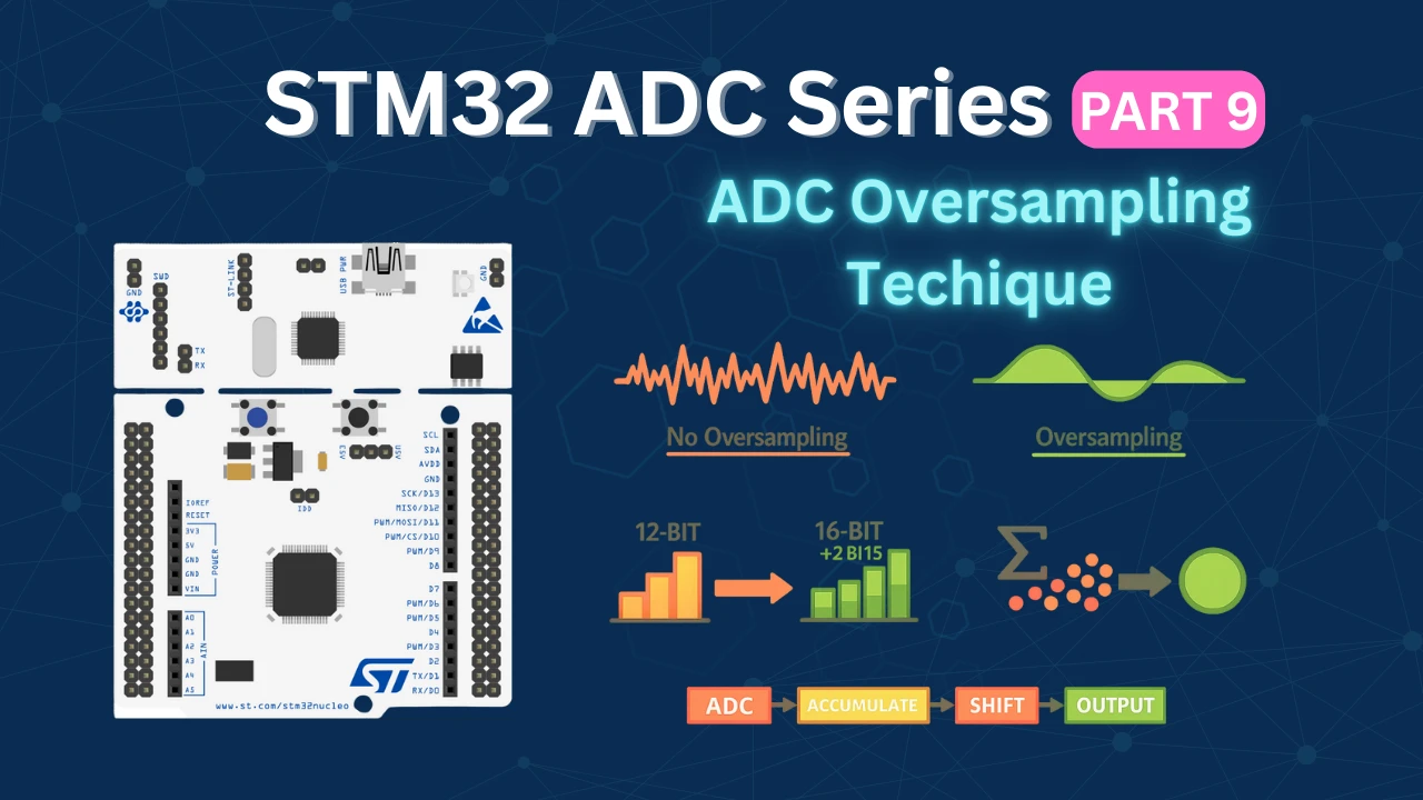
Table Of Contents
- What Is STM32 ADC Oversampling and How Does It Improve Resolution?
- STM32 ADC Oversampling CubeMX Setup: OSR, Right Shift & DMA
- Potentiometer to STM32L496 ADC: Wiring Diagram
- STM32 ADC Oversampling: HAL Code and DMA Setup
- STM32 ADC Oversampling Output: 16-bit Resolution & Conversion Timing
- STM32 ADC Hardware Oversampling — Video Tutorial
- Download STM32 ADC Hardware Oversampling Project Files
- STM32 ADC Hardware Oversampling — Frequently Asked Questions
What Is STM32 ADC Oversampling and How Does It Improve Resolution?
ADC oversampling is a technique where the ADC samples the same analog signal multiple times and then combines those samples to produce a single output value. Instead of relying on one conversion per result, the ADC accumulates several conversions internally and optionally right-shifts the result to scale it back into a usable range.
The primary reason we use oversampling is to improve measurement quality without changing hardware. Real-world analog signals always contain noise, and a single ADC conversion can fluctuate by a few LSBs even when the input voltage is stable. By oversampling, this random noise tends to average out, resulting in a smoother and more stable ADC output.
Another important benefit is increased effective resolution. With proper oversampling and right shifting, a 12-bit ADC can effectively behave like a 14-bit or even 16-bit ADC. This is extremely useful in applications such as sensor readings, battery voltage measurement, or low-level analog signals where small changes matter.
However, oversampling is not free. Since multiple conversions are required for one final result, the effective sampling rate is reduced, and the total conversion time increases. This makes oversampling ideal for slow-changing signals, but less suitable for high-speed measurements.
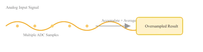
Below is a simple diagram showing how multiple ADC samples are accumulated into a single oversampled result.
How Oversampling Improves ADC Resolution (Math)
In STM32 ADCs, oversampling works by accumulating multiple ADC conversions and then optionally right-shifting the result. The increase in effective resolution depends on how many samples are accumulated.
The relationship between oversampling ratio and resolution improvement is given by:
Where:
- N = number of samples accumulated (oversampling ratio)
Example 1: 4× Oversampling
A 12-bit ADC behaves like a 13-bit ADC.
Example 2: 16× Oversampling
A 12-bit ADC behaves like a 14-bit ADC.
Example 3: 256× Oversampling
A 12-bit ADC behaves like a 16-bit ADC.
Right Shift and Final ADC Value
After accumulation, the ADC result is typically right-shifted to bring the value back into a usable range:
In CubeMX:
- Oversampling Ratio = number of samples accumulated
- Right Bit Shift = scaling factor to match the desired resolution
For example:
- Oversampling ratio = 16
- Right shift = 2 bits
This configuration yields a 14-bit effective result from a 12-bit ADC while keeping the output properly scaled.
STM32 ADC Oversampling CubeMX Setup: OSR, Right Shift & DMA
Before diving into the code, we need to configure the ADC and related peripherals using STM32CubeMX. In this section, we’ll go through the essential CubeMX settings required to make ADC oversampling work as expected.
Clock Configuration
Below is the image showing the clock configuration for STM32L496ZG.
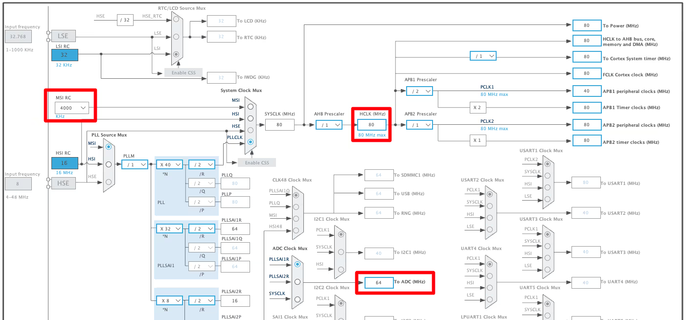
I have configured the system clock to run at maximum 80MHz. The ADC is also configured to run at 64MHz.
ADC Configuration
Below is the image showing the ADC configuration.
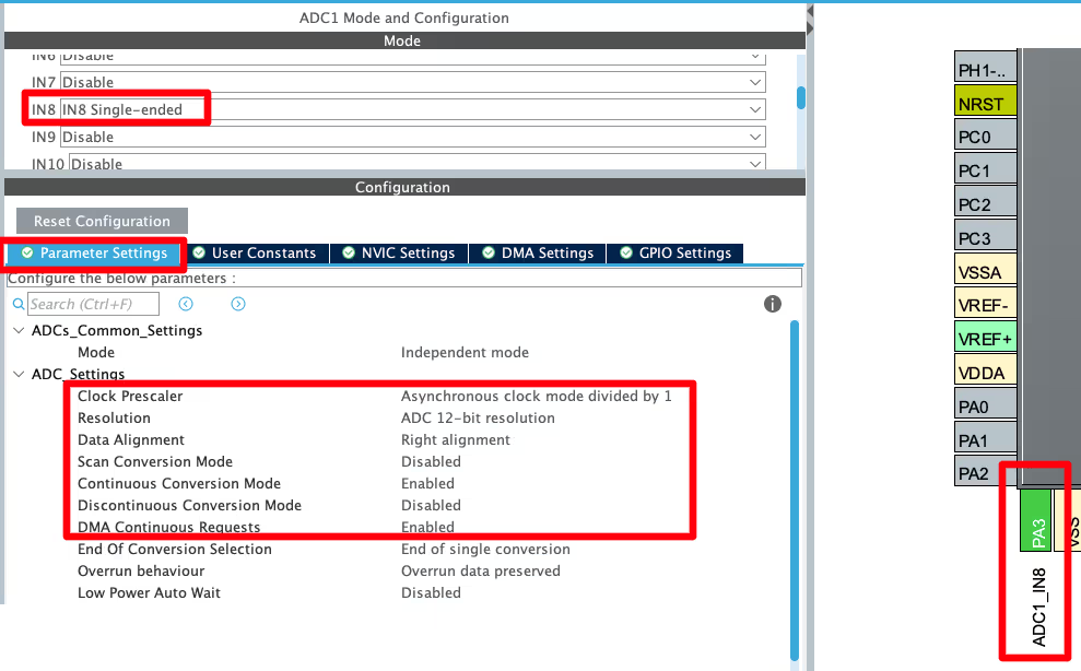
- I have configured the ADC1 CH8, which is connected to pin PA3.
- The clock prescaler is set to 1, so the ADC clock is still at 64MHz (64MHz/PSC).
- The Resolution is set to 12-bit. The extra samples we take, will be accumulated on 12-bit.
- The continuous conversion mode is enabled, so the next conversion will automatically start once the previous conversion is over.
- The DMA continuous request is enabled, so the DMA will fetch the data from the channel continuously.
ADC Oversampling configuration
Below is the image showing the oversampling and channel configuration of the ADC.
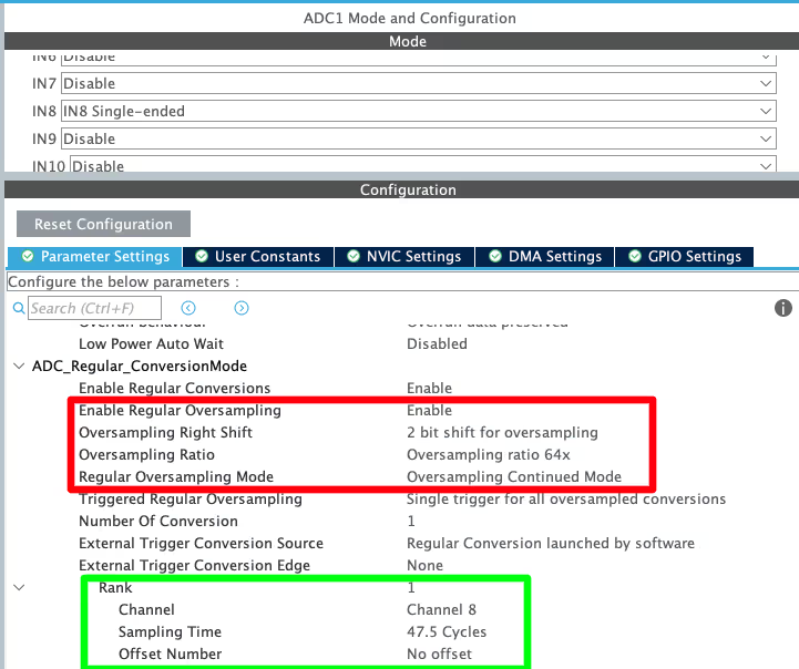
Here we will first enable the oversampling for the Regular channels. As I mentioned, below is the formula to calculate the oversampling bit width.

Here I am choosing the OSR as 64. Therefore 64 samples will be collected for each trigger (software start). The Right shift (M) is set to 2. This will result in the bit width of 16 bits.
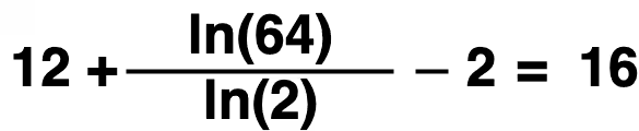
As I already mentioned, the STM32L496 has 16-bit ADC Data register, therefore we can not have the bit width higher than this value. Therefore the bit shift (M) and OSR should be selected in a way that the bit width is not higher than 16 bits.
The sampling time for the Channel 8 is set to 47.5 Cycles. With the ADC clock of 64 megahertz, the total time to convert the channel should be as shown below.
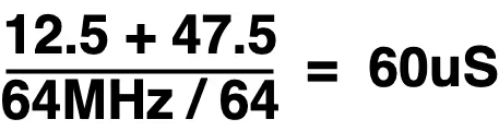
- Here 12.5 is the ADC clock for 12-bit Resolution.
- 47.5 is the sampling time we selected.
- 64MHz is the ADC clock.
- 64 is the OSR we selected.
The total conversion time for channel 8 should be 60uS. We will measure it in the analyzer.
ADC DMA Configuration
Below is the image showing the ADC DMA Configuration.
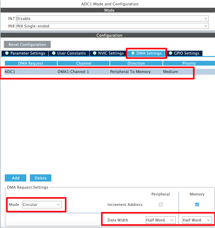
The DMA is configured in the Circular mode, so that it can work continuously. The data width is set to 16-bit.
Potentiometer to STM32L496 ADC: Wiring Diagram
Below is the image showing the connection used in this project.
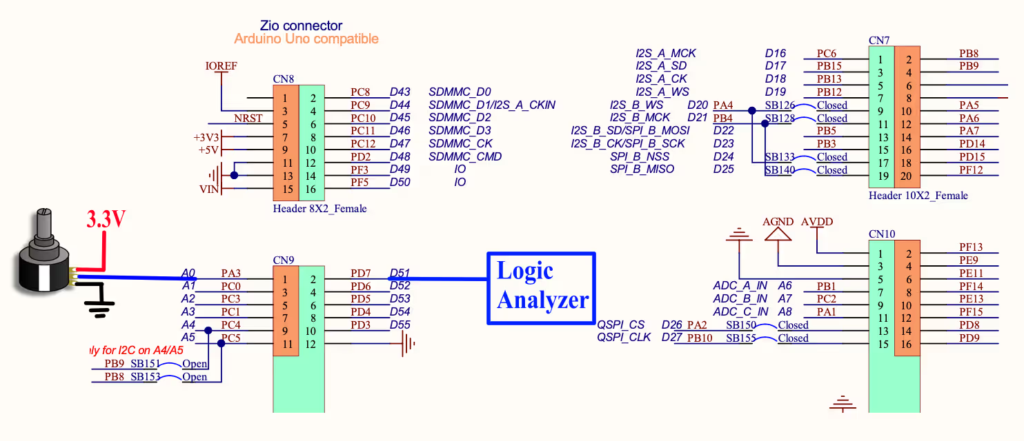
The potentiometer is connected to 3.3V with the MCU. The output pin of the potentiometer is connected to the pin PA3 (ADC1 CH8). I am going to use the pin PD7 toggle to measure the ADC conversion time, therefore it is connected to the Logic Analyzer.
STM32 ADC Oversampling: HAL Code and DMA Setup
There is nothing special in the programming section to make the oversampling work. We will simply start the ADC in the DMA mode.
uint16_t ADC_VAL = 0;

void HAL_ADC_ConvCpltCallback(ADC_HandleTypeDef *hadc)
{
    HAL_GPIO_TogglePin(GPIOD, GPIO_PIN_7);
}

int main(void)
{
  ....
  ....

  HAL_ADC_Start_DMA(&hadc1, &ADC_VAL, 1);
  while (1)
  {
  }
}Here inside the main function, we will start the ADC in the DMA mode. The converted data will be stored in the ADC_VAL variable.
Once the conversion is finished, an interrupt will trigger and the conversion complete callback is called. Inside the callback we will toggle the pin PD7. This is to measure the conversion time of the ADC.
STM32 ADC Oversampling Output: 16-bit Resolution & Conversion Timing
Below is the gif showing the ADC_VAL in the live expression.
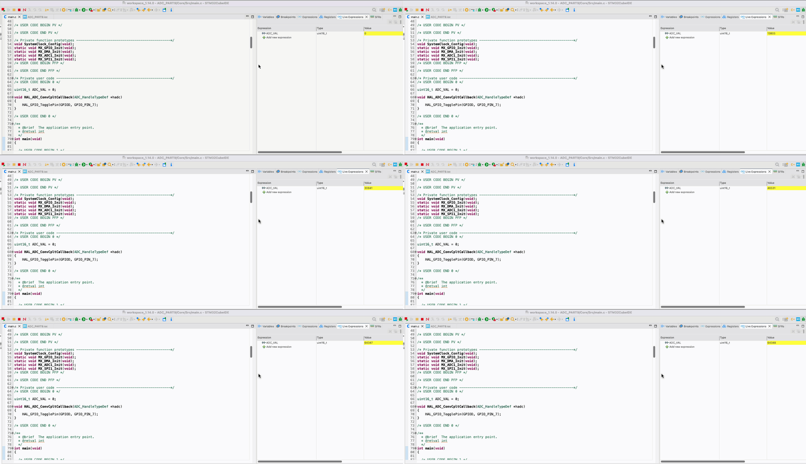
You can see in the gif above, as the potentiometer is rotated, the ADC_VAL is increasing. The interesting thing is that the maximum value of this variable is around 65000.
The STM32L496 supports a maximum of 12-bit ADC resolution. With 12-bit resolution, the maximum value of the variable should have been 4095. But because of oversampling, we are able to increase the resolution to 16-bit and that is why the value is reaching 65000.
Below is the image showing the sampling time as measured by the pin PD7.

As you can see above, the pin toggles every 60us. This is exactly the same time as we calculated using the formula.
The point is, Oversampling increases the number of samples taken per trigger by the factor OSR but it also reduces the overall sampling frequency by same factor. Hence we need to take in consideration the OSR factor while calculating the sampling or conversion frequency.
STM32 ADC Hardware Oversampling — Video Tutorial
Watch the complete walkthrough of this tutorial — understanding oversampling math and resolution improvement, configuring OSR and right bit shift in CubeMX for STM32L496, writing the DMA-based HAL code, and verifying the 16-bit output and conversion timing on a logic analyzer.
Download STM32 ADC Hardware Oversampling Project Files
Complete CubeMX project for the STM32L496, including ADC oversampling configuration with 64× OSR, DMA circular mode, and HAL code to verify 16-bit effective resolution. Free to download — support the work if it helped you.
STM32 ADC Hardware Oversampling — Frequently Asked Questions
Conclusion
In this tutorial, we covered how STM32 ADC hardware oversampling works and how to configure it using CubeMX on the STM32L496. We walked through the oversampling math, selected a 64× OSR with a 2-bit right shift to achieve 16-bit effective resolution from a 12-bit ADC, configured DMA in circular mode, and verified the output in the debugger. We also measured the actual conversion time using a logic analyzer and confirmed it matched the calculated 60µs.
Oversampling is a practical technique for any application where noise reduction or higher resolution matters — battery monitoring, precision sensor readings, or slow-changing analog signals. It requires no external hardware changes and the ADC handles all accumulation and shifting internally, leaving the CPU free. The only cost is a reduced effective sampling rate proportional to the OSR, which makes it unsuitable for high-speed measurements but ideal for anything that changes slowly.
In the next tutorial, we will look at the ADC reference voltage in STM32 — how VREFINT and VREF+ work, why the reference voltage directly affects ADC accuracy, and how to measure VDD or a custom external reference to ensure your ADC readings stay correct even when supply voltage changes. If you found this tutorial useful, stay tuned for that one.
Browse More STM32 ADC Tutorials
STM32 ADC Multiple Channels with Circular DMA: CubeMX Setup & HAL Code
STM32 ADC Multiple Channels Without DMA: CubeMX Setup & HAL Code
STM32 ADC Conversion Time: Formula, Calculation & Frequency Explained
STM32 ADC External Trigger with Timer: CubeMX & HAL Guide
STM32 ADC Injected Conversion Mode: Triggered & Auto Injection
STM32 ADC Reference Voltage: VREFINT, VREF+ & VREFBUF
STM32 ADC Differential Mode: Setup, CMV, and HAL Code Guide

Subscribe
Login
0 Comments
Newest