


Home ▸ STM32 Tutorials ▸ ADC Series ▸
Updated On: April 30, 2026
STM32 ADC Reference Voltage: VREFINT, External VREF+ & VREFBUF
Every ADC reading on STM32 is a ratio — the input voltage divided by the reference voltage, scaled to the ADC’s bit depth. If your reference is 3.3V and your supply drops to 2V, the ADC will report the maximum digital value for a 2V input, and your code will calculate 3.3V. That error doesn’t come from the ADC — it comes from using the wrong reference.
This tutorial covers three ways to handle the ADC reference voltage on STM32. First, using the internal VREFINT to measure actual VDD on the F446RE Nucleo — essential for battery-powered designs where supply voltage varies. Second, applying a custom external VREF+ on the STM32H750 to optimize ADC resolution for lower-voltage sensors. Third, using the on-chip VREFBUF peripheral to generate a stable precision reference internally without any external hardware. All three include CubeMX configuration, calibration-aware HAL code, and verified results in the debugger.
This is Part 10 of the STM32 ADC series. You can go through the other parts of this series, here are the links:
- STM32 ADC Conversion Time & Frequency Explained
- ADC External Trigger Source Selection
- ADC Injected Conversion Mode
- STM32 ADC Hardware Oversampling
- ADC in Differential Mode
STM32 ADC Reference Voltage: How It Affects Accuracy
The ADC (Analog-to-Digital Converter) in STM32 microcontrollers converts an analog signal into a digital value. This conversion process depends on a reference voltage, which defines the maximum input level the ADC can measure. In simple terms, the reference voltage (VREF) sets the upper limit of the ADC input range. Any input voltage equal to VREF is converted to the maximum digital output (e.g., 4095 for a 12-bit ADC), while 0V corresponds to a digital output of zero.
Importance of Reference Voltage in ADC Conversions
The accuracy and resolution of an ADC reading are directly tied to the chosen reference voltage. If the reference voltage is unstable or noisy, the resulting ADC values will also fluctuate. For example, with a 12-bit ADC and a 3.3V reference, the smallest step size (LSB) is:
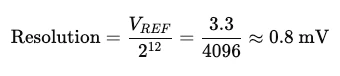
This means every ADC count represents about 0.8 mV of input change. If VREF drifts, this resolution is no longer reliable. Therefore, a clean and stable reference voltage is crucial for precise sensor measurements, battery monitoring, or any analog signal processing.
Internal vs External Reference Voltage
STM32 devices provide two ways to define the ADC reference voltage:
- Internal Reference Voltage (VREFINT):
STM32 includes a built-in, factory-calibrated reference (typically 1.2V). It is highly stable and useful for calibration tasks, such as measuring VDD or verifying ADC accuracy. However, since it is fixed, it may not cover the full input range for certain applications. - External Reference Voltage (VREF+ Pin):
Many STM32 MCUs allow an external reference voltage to be supplied through the VREF+ pin. This gives designers flexibility to use a high-precision voltage source, especially in applications that demand very accurate ADC measurements. For instance, using a 2.5V precision reference IC can significantly improve measurement consistency.
In practice, the choice between internal and external reference voltage depends on the application requirements. For general-purpose tasks, the internal reference is often sufficient. But for high-precision measurements, an external reference is usually the preferred option.
STM32 ADC Reference Pins: VREF+, VDDA, VREFINT, and VREFBUF
The availability of Vref pin is needed to provide the external reference voltage. While some MCUs have a separate Vref pin, others has it connected with the VDDA. We will see both types in this tutorial.
Let’s first see the types of voltages related to analog circuitry in STM32.
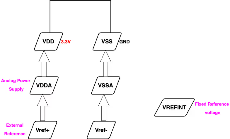
VDD and VSS are the main supply voltages. Most of the STM32 MCUs can run between 1.8V ~ 3.3V VDD. When powered normally, they run at 3.3V.
VDDA and VSSA is the separate analog supply and it is used to power the analog circuits in the MCU. Some of the STM32 MCUs has separate pins for VDDA/VSSA, but almost in all the development boards it is connected to the VDD. Although there is an option to make some hardware modification to separate these pins from the VDD.
Vref+ and Vref- are used to provide external reference voltage. These pins are also not available in all the MCUs, but wherever they are available, they are tied to VDDA by default. We again have an option to separate them from VDDA by making some hardware changes.
VREFINT is the fixed internal reference voltage. This voltage does not vary with the VDD and remains fixed even if the VDD drops to 1.8V. Hence it can be used to measure the voltage supply on the Vref+ pin or even the VDD, if the Vref+ is connected to VDD.
The parameters like availability of physical Vref+ pin, its connection with VDDA or VDD changes according to the design of the development board. For the same MCU, one dev board can have the Vref+ tied to the VDDA to VDD, while the other could have a separate Vref+ and a separate VDDA. Therefore while focussing on the MCUs, we will also see the schematic of the dev board.
Measuring VDD with VREFINT on STM32F446RE
Let’s start with the Nucleo F446RE. Below is the image from the datasheet of F446RE showing the pin availabilities in different MCUs.
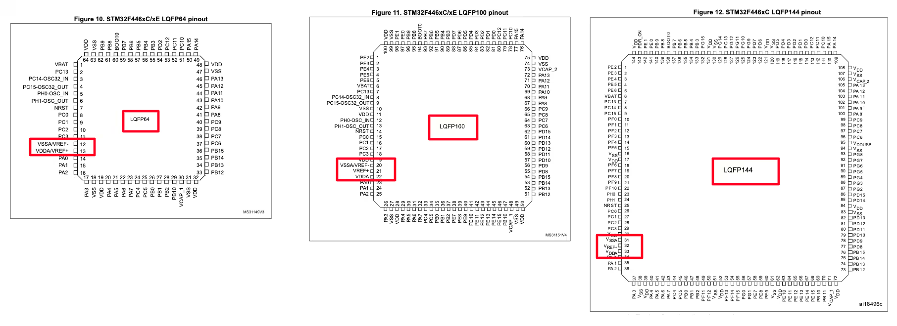
As you can see above:
- On the 144-pin STM32 package, VREF+, VDDA, and VSSA are all available as separate pins.
- In contrast, the 100-pin package exposes only VREF+ and VDDA as individual pins.
- For the Nucleo F446RE, which uses the LQFP64 package, VREF+ is internally connected to VDDA, so they are not separate.
Below is the image from the schematic of the nucleo F446RE.
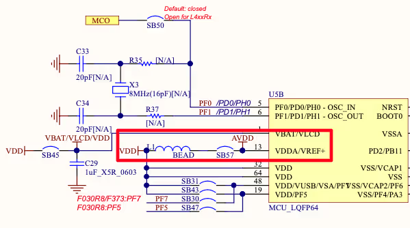
Although VDDA/VREF+ is a separate pin on the Nucleo F446, it is connected to VDD in the schematic above. You could separate it by removing the SB57 jumper, allowing an independent external reference voltage.
In this tutorial, we won’t modify the board. Instead, we will vary VDD, which automatically varies VDDA and VREF+ because they are tied together. The internal reference voltage (VREFINT) can then be used to measure VREF+, which effectively allows us to measure VDD directly.
Why Measuring VDD is Important
- Scenario: The MCU is powered by a 3.3V battery.
- ADC Reference: ADC uses VDD (3.3V) as the reference voltage.
- Problem: As the battery discharges, VDD drops (e.g., to 2V).
- If the ADC input is 2V, the ADC output will give the maximum digital value.
- Using the old 3.3V reference in calculations would incorrectly interpret the input voltage as 3.3V.
Solution
- Periodically measure VDD using the internal reference (VREFINT).
- Update the ADC formula with the current VDD:

Here, VREF = measured VDD. This ensures accurate voltage readings even as battery voltage changes.
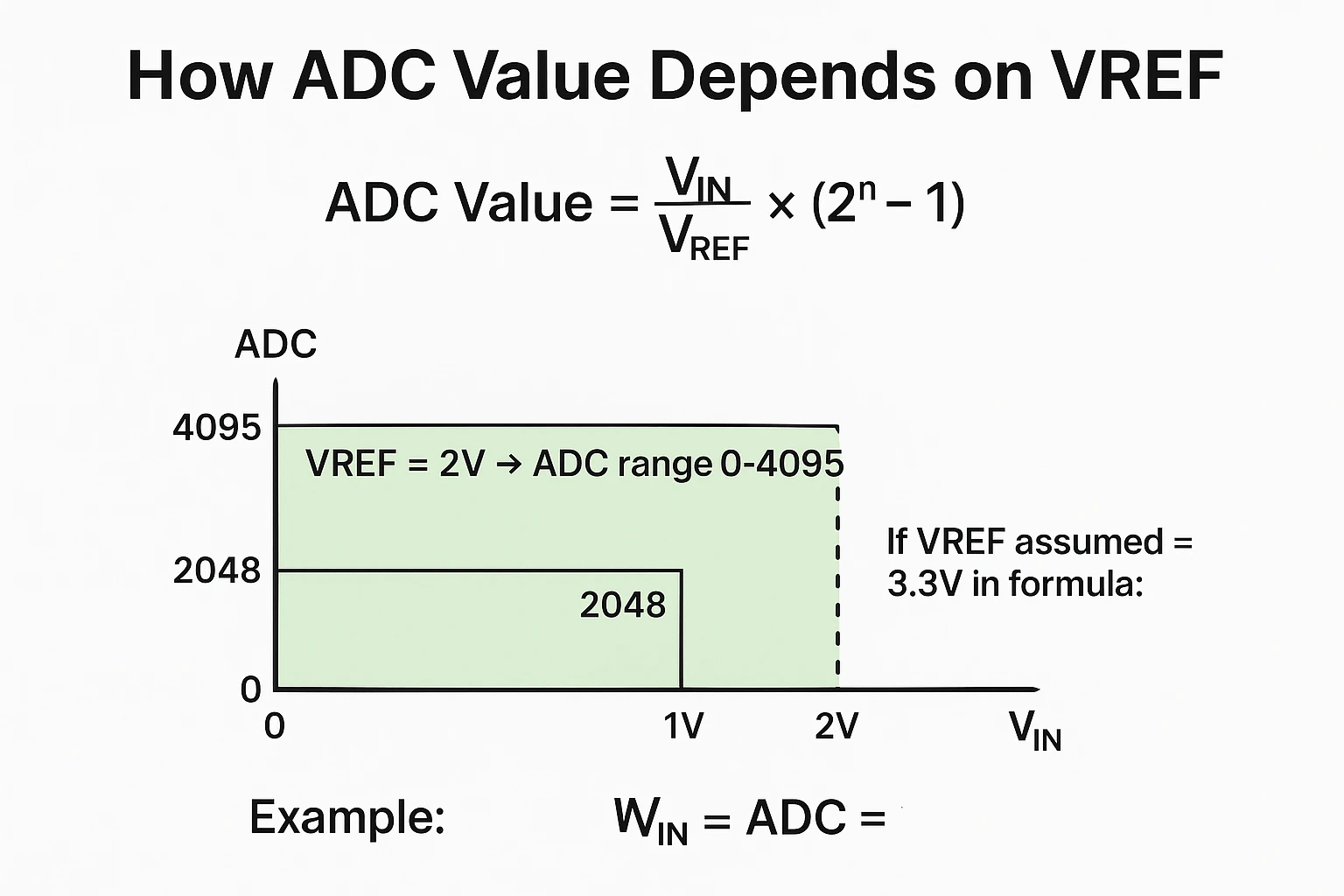
How ADC Value Depends on VREF
The ADC output is calculated using: 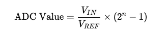
- VIN = input voltage
- VREF = reference voltage (VREF+)
- n = ADC resolution (12-bit → 4096 steps)
Example:
- Suppose VREF=2VVREF = 2VVREF=2V, 12-bit ADC:

- Input voltage VIN = 2V = 2V → ADC output = 4095 (maximum).
- If we assume VREF = 3.3V in calculations:
- The 2V input is incorrectly interpreted as 3.3V.
CubeMX Configuration (F446RE)
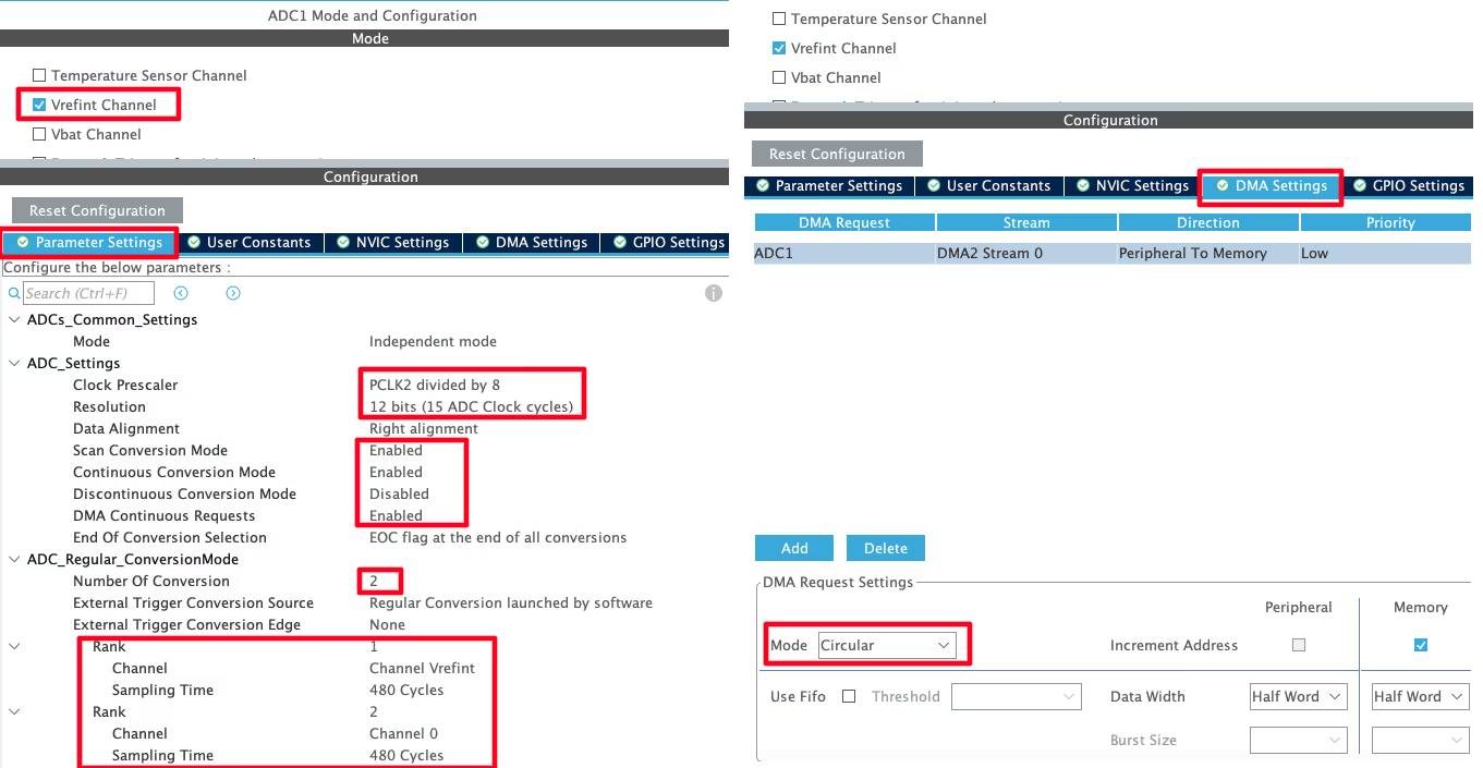
I have enabled the Vrefint channel in ADC1. There is another channel (channel 0) configured as well to measure the input voltage. I have enabled DMA, so multiple conversions can be done.
While configuring the Vrefint channel, the care must be taken to choose the sampling time. As per the datasheet of the MCU, the sampling time for this channel should be at least 10us.
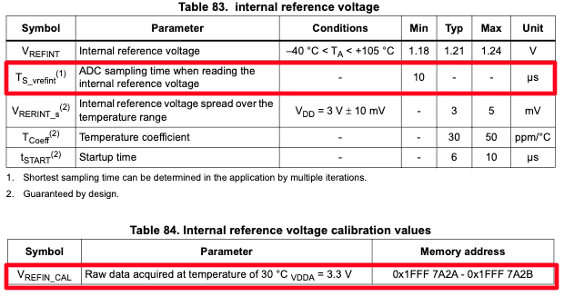
As shown in the image above, the Vrefint is around 1.21V. There is also calibration data for the internal reference voltage stored in the memory. The calibration was done at VDDA = 3.3V.
VREFINT Example Code (F446RE)
uint16_t ADC_VAL[2];
int voltage;
int vref = 0;
#define Vref_CAL *VREFINT_CAL_ADDRThe array ADC_VAL[2] will be used to store the Raw ADC values. The variable vref will store the reference voltage or VDD (in this case) whereas the variable voltage will store the ADC input voltage on channel 0.
The Vref_CAL will fetch the internal reference calibration data from the memory.
int main ()
{
....
HAL_ADC_Start_DMA(&hadc1, ADC_VAL, 2);
while (1){}
}Inside the main function we will simply start the ADC in DMA mode. The Raw data will be stored in the array ADC_VAL and here we are converting 2 channels.
Once both the conversions are finished, an interrupt will trigger and the HAL_ADC_ConvCpltCallback will be called.
void HAL_ADC_ConvCpltCallback(ADC_HandleTypeDef *hadc)
{
vref = 3300*Vref_CAL/ADC_VAL[0];
voltage = ADC_VAL[1]*vref/4095;
}Inside this callback we will first calculate the Vref/VDD using the calibrated value. The calibration was done at 3.3V, hence the value 3300 is used here.
Then using this Vref we will calculate the input voltage to the ADC.
Result: VREFINT Measurement (F446RE)
In order to provide the variable supply voltage to the nucleo F446, we need to first remove its main supply from the ST link.

The Highlighted Jumper on the nucleo board allows it to receive the power from the ST link. So we need to remove this jumper and then provide supply on the 5V pin of the board. You can provide it on any 5V pin of the board.
Below are the images showing the result of the project. Here I am providing the supply voltage of 2V to the nucleo board. You can see the Vref is also showing the same value around 2000mV.
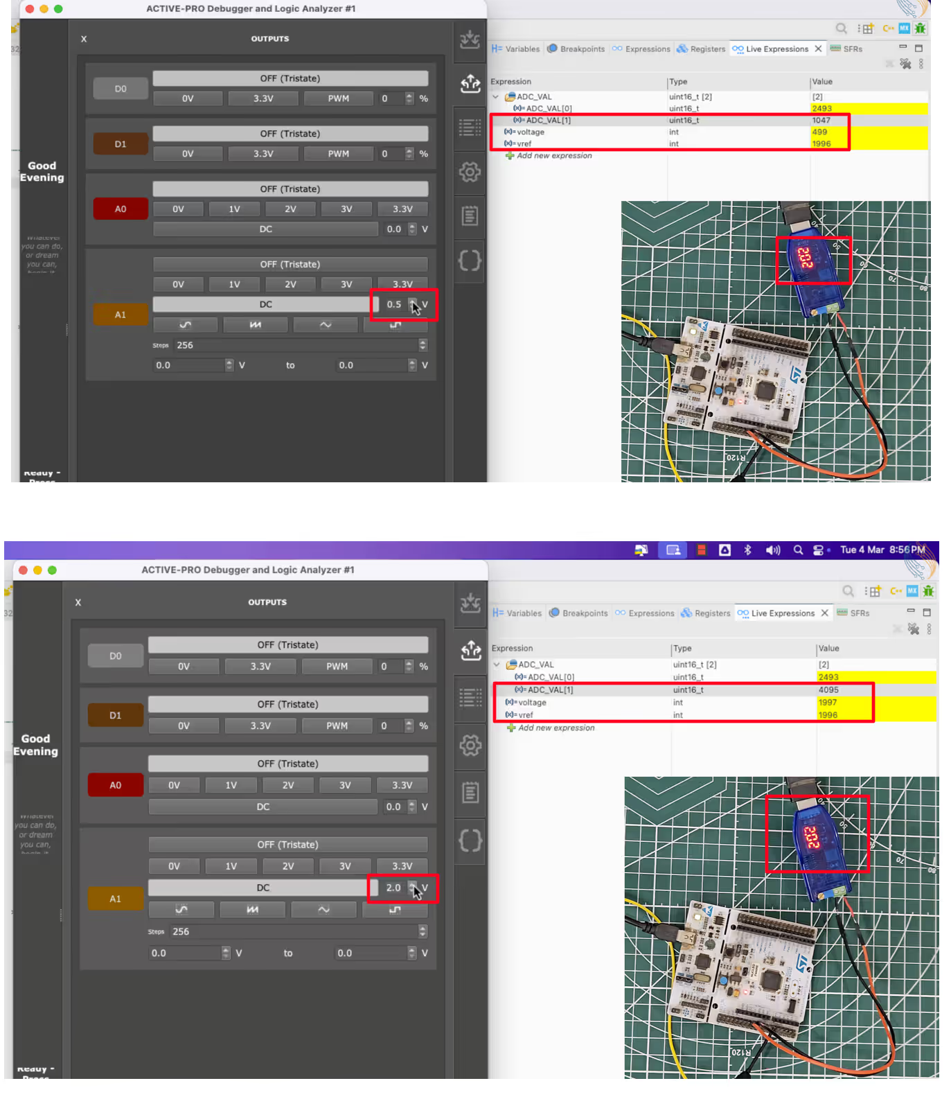
- The first image shows when the ADC input voltage is 0.5V, the live expression shows the same voltage 499mV. Also note that the ADC Raw value is 1047 for this 0.5V input.
- The second image shows when the ADC input voltage is 2V, the live expression shows the same voltage 1997mV. The ADC Raw value is 4095 for this 2V input.
The ADC in STM32 is typically a 12-bit converter, which means it produces digital values ranging from 0 to 4095. These values correspond to the input voltage relative to the reference voltage (VREF).
For example, if the reference voltage is 2V, the ADC output will span the full range (0–4095) for input voltages between 0V and 2V. This means that even a small change in input voltage—for instance, a 2V variation—can result in the ADC value jumping from 0 to 4095.
Now, imagine we assume a fixed reference voltage of 3.3V in our calculations, without actually measuring VREF. If the real input is 2V, the ADC will still output the maximum digital value (4095) because it’s scaled to the actual VREF (2V). However, if we calculate the input voltage using 3.3V as the reference, the formula will incorrectly interpret the 2V input as 3.3V.
In other words, not accounting for the actual reference voltage leads to significant measurement errors, especially when VREF varies due to factors like battery voltage drops or an unmodified development board. This is why measuring VREF (or VDD when VDDA/VREF+ is tied to it) is critical for accurate ADC readings.
We can also use this method to monitor the VDD and set a kind of alarm system to indicate the low voltage of the battery.
External VREF+ and VREFBUF on STM32H750
Using a Custom External VREF+ (H750)
We saw that on Nucleo F446 the VREF pin is connected to the VDDA, which is then connected to the VDD. Hence we were able to measure the VDD using the Vrefint channel. Now we will take a look at the H750 Based Custom Development Board. It has separate pins for Vref and VDDA, therefore we will use the Vrefint to calculate the actual variable Vref this time, while keeping the VDD constant.
Below is the image showing the schematic of this board.
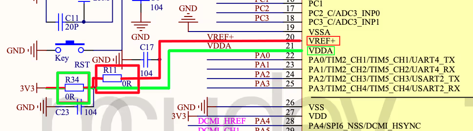
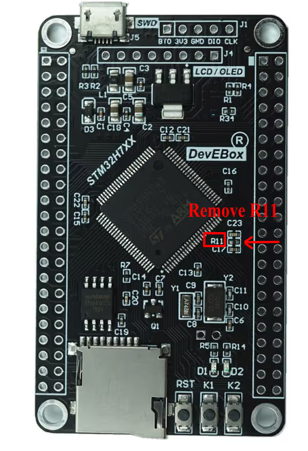
The Red Line shows the connection of the Vref+ to 3.3V. Whereas the Green line shows the connection of VDDA to 3.3V. There is a 0 Ohm Resistor (R11), which can be removed to make the Vref+ an independent pin. I did the same on this board and now the Vref+ can be used to provide an external reference voltage for the ADC.
CubeMX Configuration (H750)
Below is the configuration for Vrefint channel.

The Vrefint channel is available in ADC3. I have disabled the continuous conversion mode and we will read this channel in the blocking mode.
While configuring the Vrefint channel, the care must be taken to choose the sampling time. As per the datasheet of the MCU, the sampling time for this channel should be at least 4.3us.

As shown in the image above, the Vrefint is around 1.216V. There is also calibration data for the internal reference voltage stored in the memory. The calibration was done at VDDA = 3.3V.
Below is the image showing the configuration for ADC input channel.
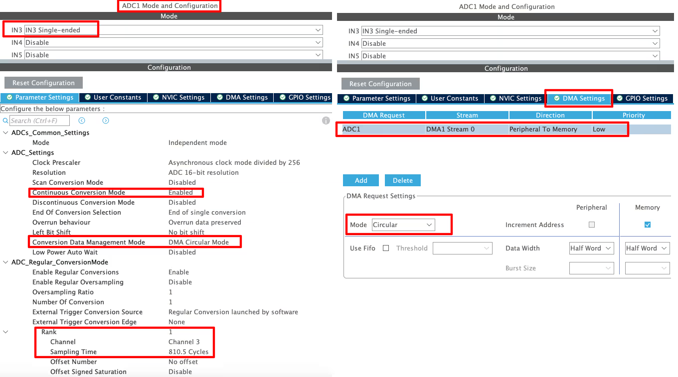
I have enabled ADC1 channel 3 in single ended mode. We will provide the variable input voltage on this pin. The ADC is configured in Circular DMA mode, so the data reading will continue on its own.
VREFINT Example Code (H750)
uint16_t ADC_VAL[2];
int voltage;
int vref = 0;
#define Vref_CAL *VREFINT_CAL_ADDR
The array ADC_VAL[2] will be used to store the Raw ADC values. The variable vref will store the reference voltage or VDD (in this case) whereas the variable voltage will store the ADC input voltage on channel 0.
The Vref_CAL will fetch the internal reference calibration data from the memory.
volatile int isDone =0;
void HAL_ADC_ConvCpltCallback(ADC_HandleTypeDef *hadc)
{
	isDone = 1;
}When the ADC finished the conversion and the data is transferred via the DMA, the ConvCpltCallback will be called. Inside this callback we will simply set the variable isDone. The data will be processed in the while loop.
int main(void)
{
  ....
  ....
  HAL_ADC_Start_DMA(&hadc1, &ADC_VAL[0], 1);
  while (1)
  {
	  HAL_ADC_Start(&hadc3);
	  HAL_ADC_PollForConversion(&hadc3, 10);
	  ADC_VAL[1] = HAL_ADC_GetValue(&hadc3);
	  HAL_ADC_Stop(&hadc3);
	  vref = 3300*vref_cal/ADC_VAL[1];
	  if (isDone)
	  {
		  voltage = ADC_VAL[0]*vref/65535;
		  isDone = 0;
	  }
	  HAL_Delay(250);
  }
}Inside the main function, we will start the ADC1 in the DMA mode. The ADC Raw value will be stored in the 0th position of the ADC_VAL array.
Inside the while loop, we will read the ADC channel 3 in the blocking mode. The ADC Raw data for this Vrefint channel will be stored in the 1st position of the ADC_VAL array.
Then calculate the Vref using the calibrated value. The calibration was done at 3.3V, hence the value 3300 is used here.
Then we will check if the ADC1 has finished converting channel 3. If it did, we will calculate the input voltage using the vref value we just calculated.
Basically we are first calculating the Vref using internal reference voltage, and then using this Vref as the reference voltage for the ADC input. Therefore if the Vref varies on Vref+ pin, our ADC input will be measured as according to the updated voltage.
Result: External VREF+ Measurement (H750)
The following images demonstrate the results of measuring the internal reference voltage (VREFINT) and the ADC input on the STM32 H750. These results validate both the ADC configuration and the accuracy of the measured voltages.
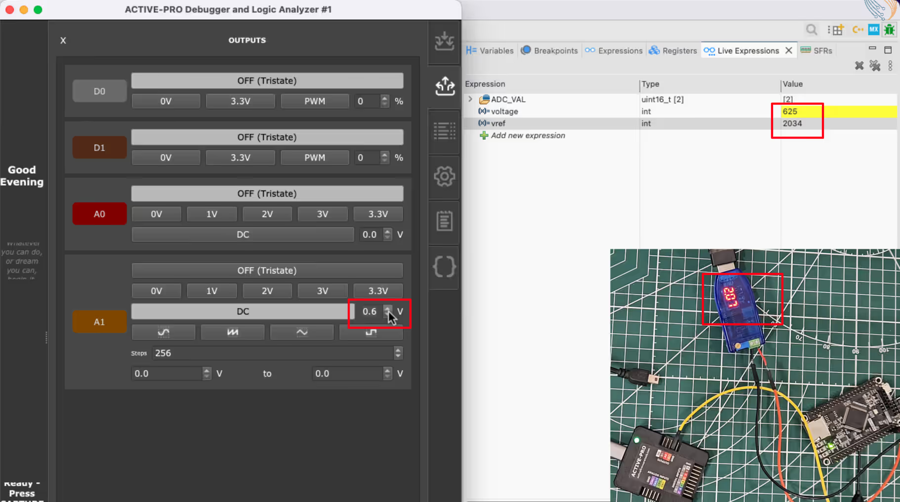
In the image below, the external supply on the VREF+ pin is approximately 2V. The live measurement confirms this, showing the voltage variable correctly reflecting the applied voltage. When the ADC input is 0.6V, the voltage variable reads 625 mV, demonstrating accurate conversion and calibration.
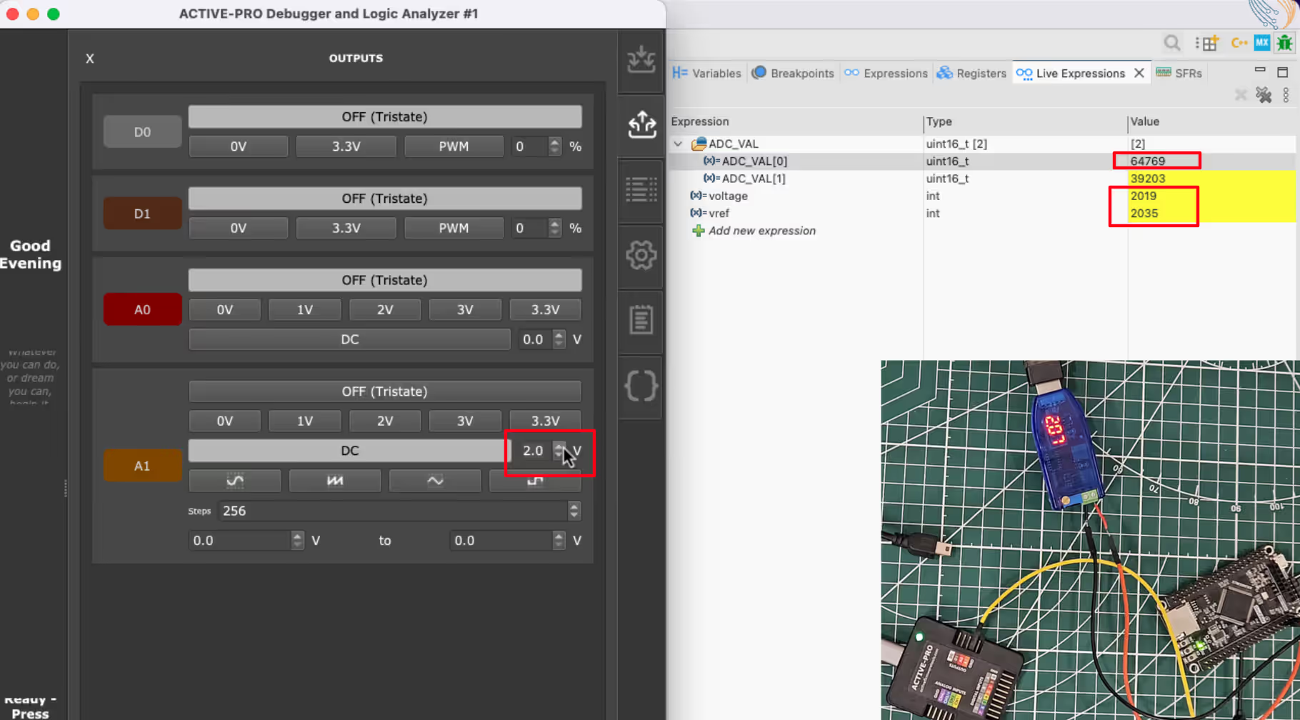
When the input voltage is increased to 2V, the live voltage variable matches the input, confirming that the ADC accurately reflects the applied voltage. The corresponding raw ADC value reaches near the maximum of 65535, showing full utilization of the 16-bit ADC range.
Using a custom reference voltage is particularly important when working with sensors that output voltages lower than the standard 3.3V. For example, if a sensor outputs between 0 and 2V, setting VREF+ to 2V ensures the ADC uses its full resolution for this input range. This maximizes measurement precision and avoids wasting ADC steps.
While it is possible to use a standard 3.3V reference for a 0–2V sensor, doing so would limit the effective resolution to less than two-thirds of the ADC’s full range, reducing accuracy. Custom reference voltages allow you to scale the ADC input range optimally for your specific sensor or application.
Generating a Custom VREF with VREFBUF on STM32
Some of the STM32 MCUs has a peripheral to generate the custom Reference voltage on the Vref+ pin. This can be achieved by using the peripheral Analog Voltage Reference Buffer, VREFBUF.
The VREFBUF is supplied via the VDDA pin. When enabled, it can provide a reference voltage in the range of: 1.65V, 1,8V, 2.048V or 2.5V. The VREFBUF can be used to provide an analog voltage reference for:
- ADC internal peripheral
- External components through the dedicated VREF+ pin.
The VREFBUF can be left unused. In this case, an external voltage regulator can provide reference voltage to VREF+ pin.
Even though the VREF+ pin can be used to provide the voltage to external component, note that the current supply in very limited on this pin, approximately around 4mA.
VREFBUF CubeMX Configuration
Below is the image showing the configuration for the VREFBUF.
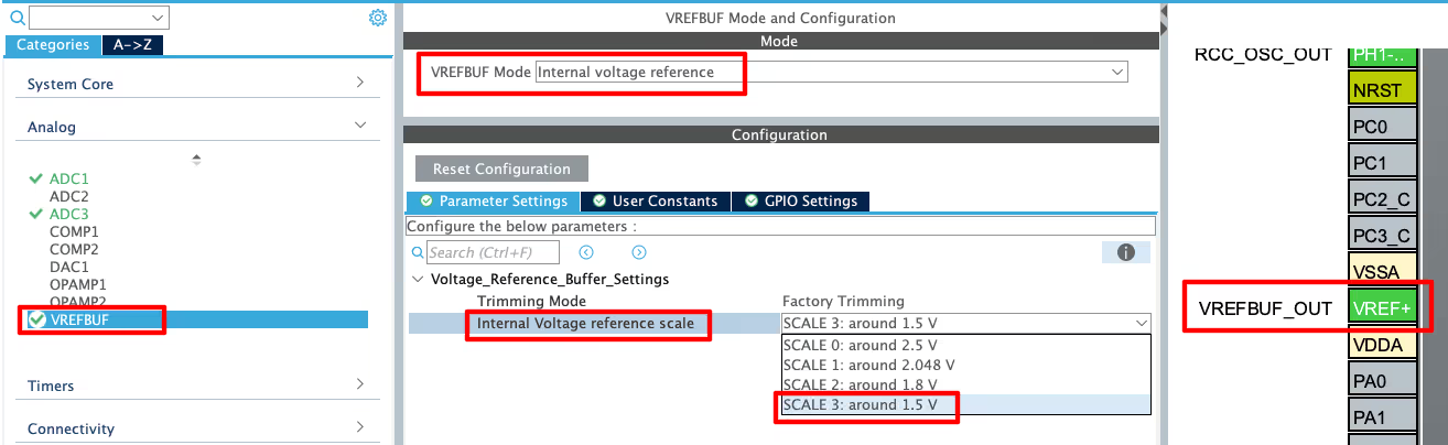
I have configured the VREFBUF Mode as Internal Voltage Reference. In this mode the VREFBUF generates a custom reference voltage on VREF+ pin.
There are multiple voltage output options available on this MCU. I am selecting the 1.5V Output Voltage.
Note that the VREF+ pin is automatically configured as VREFBUF_OUT. We can even use this pin to power our sensor, but remember that the current output is very low (around 4mA).
VREFBUF Result
Although we do not need to measure the VREF now, since we are using VREFBUF to generate it. But I am keeping the code same, so that we can get an idea if the voltage generated is same.
Also I have removed the external power supply from this Vref+ pin.
Below is the image showing the result of this project.
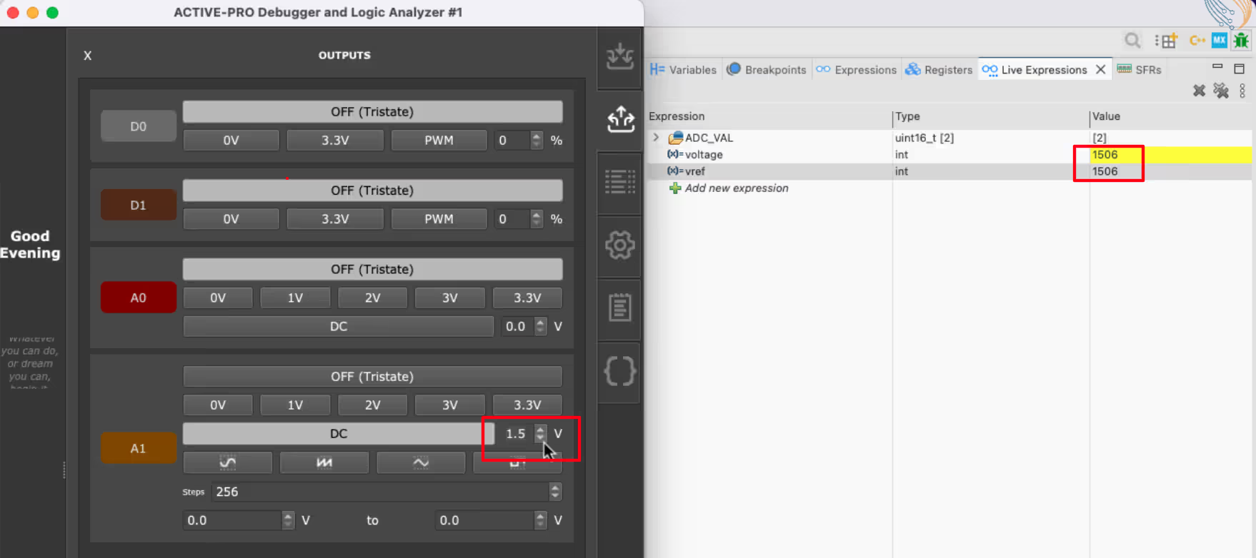
You can see the Vref is measured as 1500mV, which is the same as generated by the VREFBUF. Also note that we are able to measure the input voltage using this internally generated reference voltage.
STM32 ADC Reference Voltage — Video Tutorial
This video walks through all three reference voltage approaches on STM32 — using VREFINT to measure variable VDD on the F446RE Nucleo, applying a custom external VREF+ on the STM32H750 after removing the 0Ω resistor, and configuring VREFBUF to generate a 1.5V internal reference. Includes CubeMX setup, calibration-aware HAL code, and live debugger results for each method.
STM32 ADC Reference Voltage — Frequently Asked Questions
Conclusion
In this tutorial, we covered how the ADC reference voltage works in STM32 and why getting it right is essential for accurate measurements. We demonstrated three different approaches — using VREFINT to measure a variable VDD on the F446RE Nucleo, using a custom external VREF+ on the H750, and generating an internal 1.5V reference using VREFBUF. Each approach included the relevant CubeMX configuration, calibration-aware HAL code, and verified results in the debugger.
The key takeaway is that every ADC reading is relative to VREF, so if you assume a fixed 3.3V reference but the actual reference has changed, your voltage calculations will be wrong. Measuring VREFINT and using it to dynamically calculate the actual reference voltage ensures your ADC readings stay accurate even as supply voltage fluctuates — which is critical for battery-powered systems, low-voltage sensors, or any design where the supply is not rock-solid.
In the next tutorial, we will look at ADC differential mode, where the ADC measures the voltage difference between two input pins instead of a single-ended voltage relative to ground. This is particularly useful for noise rejection, current sensing, and small-signal measurements. If you found this tutorial useful, stay tuned for that one.
Download STM32 ADC Reference Voltage Project Files
Complete CubeMX projects for STM32F446RE and STM32H750, covering VREFINT-based VDD measurement, custom external VREF+, and VREFBUF configuration with calibrated HAL code. Free to download — support the work if it helped you.
Browse More STM32 ADC Tutorials
STM32 ADC Multiple Channels with Circular DMA: CubeMX Setup & HAL Code
STM32 ADC Multiple Channels Without DMA: CubeMX Setup & HAL Code
STM32 ADC Conversion Time: Formula, Calculation & Frequency Explained
STM32 ADC External Trigger with Timer: CubeMX & HAL Guide
STM32 ADC Injected Conversion Mode: Triggered & Auto Injection

Subscribe
Login
0 Comments
Newest