
Updated On: May 10, 2026
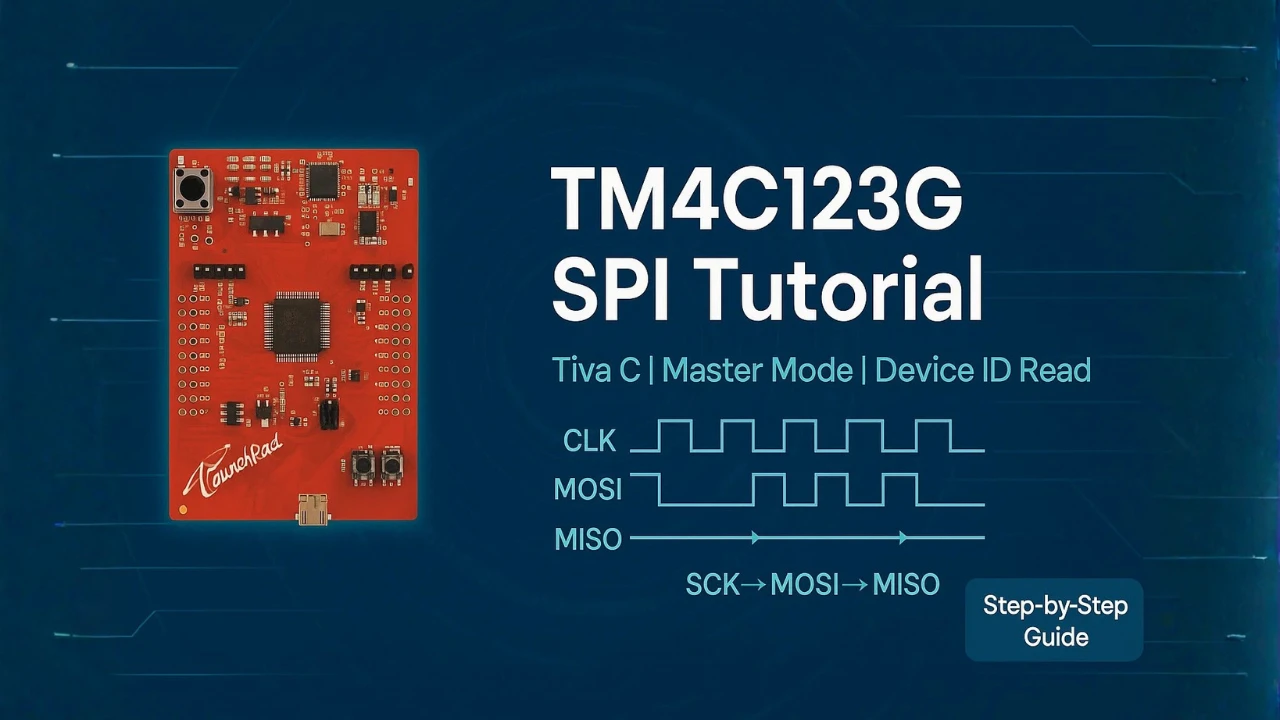
TM4C123G SPI Communication: Configure SSI0 and Read ADXL345 Device ID
SPI is one of the fastest synchronous communication protocols available on embedded microcontrollers — and on the TM4C123G Tiva C LaunchPad, it’s handled by the on-chip SSI (Synchronous Serial Interface) peripheral. This tutorial shows you how to configure SSI0 for SPI using TivaWare, wire it to a real device, and prove the bus is working with a single register read.
The test target is the ADXL345 accelerometer. We read only its fixed Device ID register (0x00), which always returns 0xE5. A correct read confirms that your pin mapping, SPI mode, clock speed, and CS handling are all correct — before you write a single line of sensor-specific driver code.
What you’ll need: TM4C123G Tiva C LaunchPad, ADXL345 breakout board, jumper wires, Code Composer Studio, TivaWare SDK, and optionally a logic analyzer.
What this tutorial covers: SPI theory and the four modes, SSI module overview and pin mapping, wiring the ADXL345, complete TivaWare SPI init code, the ADXL345 device ID read function, UART debug output, logic analyzer output, and a focused troubleshooting guide.
This tutorial is part of the TM4C123G series. Before starting, make sure you’ve completed Setting Up CCS and Building Your First TM4C123G Project and TM4C123G Clock Configuration. For other peripherals in the same series, see I2C with TivaWare, UART with VCP, and the full TM4C123G Tutorial Index.
How SPI Works
SPI (Serial Peripheral Interface) is a synchronous, full-duplex communication protocol driven by a master device — in this case, the TM4C123G. Unlike I2C, SPI needs no address arbitration and no ACK handshaking, which is why it can comfortably run at several MHz.
SPI Lines and Roles
SPI uses four signal lines:
| Line | Direction | Function |
|---|---|---|
| SCK | Master → Slave | Clock generated by the master; synchronizes every bit |
| MOSI | Master → Slave | Data from master to slave |
| MISO | Slave → Master | Data from slave to master |
| CS / SS | Master → Slave | Selects the active slave (active LOW) |
The master controls SCK and CS. Multiple slaves can share the same MOSI, MISO, and SCK lines as long as each slave has a dedicated CS line. Only the slave whose CS is pulled LOW responds.
SPI Data Frame Format and the Four Modes
A transaction begins when the master pulls CS LOW. The master then clocks bits out on MOSI and simultaneously reads bits in on MISO — full duplex, every clock cycle. The transaction ends when CS goes HIGH.
Two configuration bits define exactly when data is driven and sampled:
- CPOL (Clock Polarity) — idle state of the clock line (0 = idle LOW, 1 = idle HIGH)
- CPHA (Clock Phase) — which clock edge captures data (0 = first edge, 1 = second edge)
| Mode | CPOL | CPHA | Clock Idle | Data Captured On |
|---|---|---|---|---|
| Mode 0 | 0 | 0 | LOW | Rising edge |
| Mode 1 | 0 | 1 | LOW | Falling edge |
| Mode 2 | 1 | 0 | HIGH | Falling edge |
| Mode 3 | 1 | 1 | HIGH | Rising edge |
Always check your slave device’s datasheet to confirm which mode it requires. The ADXL345 uses SPI Mode 3.
Why Use SPI in Embedded Systems
SPI is the right choice when you need high data throughput, deterministic timing, and simple protocol overhead. It supports multi-MHz operation (limited mostly by PCB trace quality and slave device limits), requires no addressing or acknowledgment exchanges, and the master always has full control of the clock. These properties make it the dominant protocol for displays, flash memory, ADCs, DACs, and sensors like the ADXL345.
SPI on the TM4C123G: SSI Modules and Pin Mapping
The TM4C123G’s SPI hardware is called SSI (Synchronous Serial Interface). The chip includes four independent SSI modules — SSI0 through SSI3 — each capable of running SPI, TI synchronous serial, or Microwire protocols.
SSI0 to SSI3 Overview
| Module | Base Address | Notes |
|---|---|---|
| SSI0 | 0x4000.8000 | Default choice — pins on Port A, easily accessible on LaunchPad headers |
| SSI1 | 0x4000.9000 | Pins on Port F |
| SSI2 | 0x4000.A000 | Pins on Port B or D |
| SSI3 | 0x4000.B000 | Pins on Port D or F |
All four modules are fully independent and can run simultaneously at different speeds and modes — useful when your board connects multiple SPI devices that have different timing requirements.
SPI Pin Mapping Reference
| Module | CLK | FSS (CS) | RX (MISO) | TX (MOSI) | Port |
|---|---|---|---|---|---|
| SSI0 | PA2 | PA3 | PA4 | PA5 | A |
| SSI1 | PF2 | PF3 | PF0 | PF1 | F |
| SSI2 | PB4 / PD3 | PB5 / PD2 | PB6 / PD1 | PB7 / PD0 | B / D |
| SSI3 | PD0 / PF2 | PD1 / PF3 | PD2 | PD3 | D / F |
This tutorial uses SSI0 on Port A (PA2–PA5). Always confirm pin mapping against the TM4C123G datasheet or pin_map.h — alternate function assignments are fixed in silicon and cannot be reassigned freely.
Clock Speed, Mode, and Wiring Notes
Each SSI module supports selectable CPOL/CPHA (all four SPI modes), data frames from 4 to 16 bits, and a programmable bit rate derived from the system clock. SPI does not require pull-up resistors — lines are push-pull. Keep the following in mind for reliable communication: connect all grounds between the MCU and slave before powering up; keep MOSI, MISO, and SCK traces or wires short; and if you’re seeing signal ringing at higher speeds, add 33–100 Ω series resistors at the master-side pin.
Hardware Setup – Connecting ADXL345 to TM4C123G
The ADXL345 is a 3-axis digital accelerometer with both I2C and SPI interfaces. In this tutorial we use only its SPI interface and only its Device ID register — no motion data, no interrupts. The goal is simply to verify that the SPI bus is working end-to-end.
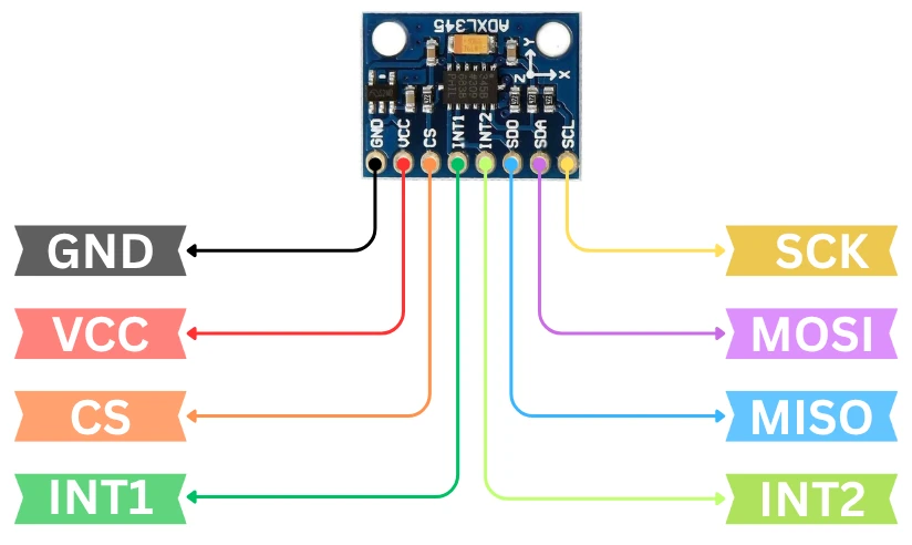
ADXL345 SPI Pinout
| Pin | SPI Function | Notes |
|---|---|---|
| VCC | Power | Connect to 3.3 V — ADXL345 is not 5 V tolerant |
| GND | Ground | Common ground with TM4C123G |
| CS | Chip Select | Active LOW — must be LOW to enable SPI mode |
| SCL | SPI Clock (SCK) | Clock driven by TM4C123G |
| SDA | MOSI | Data from TM4C123G to ADXL345 |
| SDO | MISO | Data from ADXL345 to TM4C123G |
| INT1/INT2 | Interrupt outputs | Not used in this tutorial |
Wiring Table: SSI0 to ADXL345
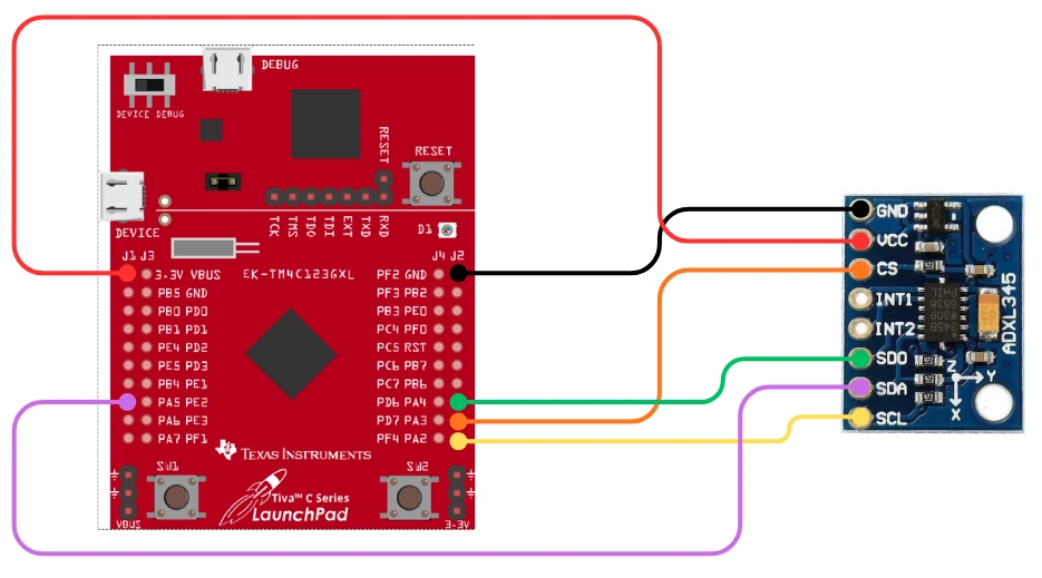
| TM4C123G Pin | ADXL345 Pin | Signal |
|---|---|---|
| PA2 | SCL | SPI Clock |
| PA3 | CS | Chip Select |
| PA5 | SDA | MOSI (master out) |
| PA4 | SDO | MISO (master in) |
| 3.3 V | VCC | Power |
| GND | GND | Ground |
Keep the wires short. For bench testing with jumper wires, 10 cm or less is ideal — longer connections at 4 MHz can introduce enough capacitance to corrupt data edges.
SPI Mode Required for ADXL345
The ADXL345 datasheet specifies SPI Mode 3 (CPOL = 1, CPHA = 1): the clock idles HIGH and data is captured on the rising clock edge. This must be matched exactly in SSIConfigSetExpClk(). Using the wrong mode will produce either zeros, all-ones (0xFF), or random garbage on the MISO line.
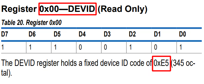
The fixed Device ID we are reading is always 0xE5. Any other return value means the configuration is wrong.
Configuring SSI0 for SPI in TivaWare
Project Setup in CCS
This tutorial assumes a CCS project created from the blinky template, as described in the TM4C123G Getting Started tutorial. Starting from a fresh blinky project:
- Delete all content from
blinky.cand rename it tomain.c - Rename
blinky_ccs.cmdtolinker.cmd - Rename the top-level project folder to your project name

Next, add basic_conf.c and basic_conf.h to the project root. These files configure the system clock (MOSC + PLL at 80 MHz) and set up SysTick as the delay timebase — see the Clock Configuration and Delay tutorials for the full explanation.

In main.c, add #include "basic_conf.h" and #include "driverlib/interrupt.h". Call systemClockConfig() as the first line of main(), and call IntMasterEnable() after all peripheral initialization to enable SysTick-based delays.
Required Header Files
#include <stdint.h>
#include <stdbool.h>
#include "inc/hw_memmap.h"
#include "driverlib/sysctl.h"
#include "driverlib/ssi.h"
#include "driverlib/gpio.h"
#include "driverlib/pin_map.h"What each header provides: <stdint.h> and <stdbool.h> give fixed-width integer types and boolean support. hw_memmap.h defines peripheral base addresses like SSI0_BASE and GPIO_PORTA_BASE. sysctl.h enables peripheral clock gating. ssi.h provides all SSI/SPI API functions. gpio.h handles pin direction and alternate function assignment. pin_map.h maps GPIO pins to their SSI alternate functions — without it, constants like GPIO_PA2_SSI0CLK are undefined.
Enable Clocks and Configure GPIO Pins
Before accessing any SSI or GPIO register, the peripheral clock must be enabled and allowed time to stabilize:
SysCtlPeripheralEnable(SYSCTL_PERIPH_SSI0);
SysCtlPeripheralEnable(SYSCTL_PERIPH_GPIOA);

while (!SysCtlPeripheralReady(SYSCTL_PERIPH_SSI0));
while (!SysCtlPeripheralReady(SYSCTL_PERIPH_GPIOA));Then assign the alternate SPI function to each pin and set their type:
GPIOPinConfigure(GPIO_PA2_SSI0CLK);
GPIOPinConfigure(GPIO_PA3_SSI0FSS);
GPIOPinConfigure(GPIO_PA4_SSI0RX);
GPIOPinConfigure(GPIO_PA5_SSI0TX);
GPIOPinTypeSSI(GPIO_PORTA_BASE, GPIO_PIN_2 | GPIO_PIN_3 |
GPIO_PIN_4 | GPIO_PIN_5);GPIOPinConfigure() tells the pin mux which alternate function to route to that pin. GPIOPinTypeSSI() then sets the electrical characteristics — drive strength, slew rate, and digital enable — appropriate for a push-pull SPI driver.
Initialize SPI Mode, Clock, and Frame Size
SSIConfigSetExpClk(SSI0_BASE,
SysCtlClockGet(), // System clock reference
SSI_FRF_MOTO_MODE_3, // SPI Mode 3 (CPOL=1, CPHA=1)
SSI_MODE_MASTER, // TM4C123G is the master
4000000, // 4 MHz SPI clock
8); // 8-bit data framesSSI_FRF_MOTO_MODE_3 selects Motorola SPI frame format with Mode 3 timing — matching the ADXL345 requirement. The 4 MHz clock is well within the ADXL345’s 5 MHz maximum and gives clean waveforms on typical jumper wire setups. Finally, enable the module:
SSIEnable(SSI0_BASE);Send and Receive Data Over SPI
SPI is always full-duplex: every byte sent produces a byte received, and every byte received requires a byte sent. TivaWare’s blocking APIs handle this simply:
// Transmit
SSIDataPut(SSI0_BASE, txByte);
// Receive
uint32_t rxData;
SSIDataGet(SSI0_BASE, &rxData);When reading a register, you must first send the command byte, discard the simultaneously-received dummy byte, then send a dummy byte to generate the clock cycles that bring back the register’s value:
uint32_t dummy, rxData;
SSIDataPut(SSI0_BASE, commandByte); // Send register address + read bit
while (SSIBusy(SSI0_BASE));
SSIDataGet(SSI0_BASE, &dummy); // Discard received byte during command phase
SSIDataPut(SSI0_BASE, 0x00); // Send dummy byte to clock in response
while (SSIBusy(SSI0_BASE));
SSIDataGet(SSI0_BASE, &rxData); // Read the register valueThis two-phase pattern — command then dummy clock — is the standard SPI register read idiom and applies to virtually every SPI sensor and memory device.
Complete SPI0_Init() Function
void SPI0_Init(void)
{
// Enable SSI0 and Port A clocks
SysCtlPeripheralEnable(SYSCTL_PERIPH_SSI0);
SysCtlPeripheralEnable(SYSCTL_PERIPH_GPIOA);

while (!SysCtlPeripheralReady(SYSCTL_PERIPH_SSI0));
while (!SysCtlPeripheralReady(SYSCTL_PERIPH_GPIOA));
// Assign SPI alternate functions to PA2-PA5
GPIOPinConfigure(GPIO_PA2_SSI0CLK);
GPIOPinConfigure(GPIO_PA3_SSI0FSS);
GPIOPinConfigure(GPIO_PA4_SSI0RX);
GPIOPinConfigure(GPIO_PA5_SSI0TX);

GPIOPinTypeSSI(GPIO_PORTA_BASE, GPIO_PIN_2 | GPIO_PIN_3 |
                                GPIO_PIN_4 | GPIO_PIN_5);
// Configure SSI0: Mode 3 master, 4 MHz, 8-bit frames
SSIConfigSetExpClk(SSI0_BASE,
SysCtlClockGet(),
SSI_FRF_MOTO_MODE_3,
SSI_MODE_MASTER,
4000000,
8);
SSIEnable(SSI0_BASE);
// Flush receive FIFO
uint32_t dummy;
while (SSIDataGetNonBlocking(SSI0_BASE, &dummy));
}The FIFO flush at the end clears any stale data left in the receive buffer — a recommended step before the first real transfer.
Reading the ADXL345 Device ID Over SPI
ADXL345 Register 0x00 and the Read Command Format
The ADXL345 encodes the operation type in the two most significant bits of the first byte sent over SPI:
| Bit 7 | Bit 6 | Bits 5:0 |
|---|---|---|
| R/W̄ (1 = Read) | MB (1 = multi-byte) | Register address |
To read a single byte from register 0x00: set bit 7 to 1 (read), leave bit 6 at 0 (single byte), and the address is 0x00 — so the command byte is 0x80.
H3: Full Read Function: ADXL345_ReadDeviceID()
uint8_t ADXL345_ReadDeviceID(void)
{
    uint32_t dummy;
    uint32_t rxData;

    uint8_t command = 0x00 | 0x80;   // Register 0x00, read bit set

    // Assert CS (PA3 LOW)
    GPIOPinWrite(GPIO_PORTA_BASE, GPIO_PIN_3, 0x00);

    // Phase 1: Send command byte, discard received dummy
    SSIDataPut(SSI0_BASE, command);
    while (SSIBusy(SSI0_BASE));
    SSIDataGet(SSI0_BASE, &dummy);

    // Phase 2: Send dummy byte, receive Device ID
    SSIDataPut(SSI0_BASE, 0x00);
    while (SSIBusy(SSI0_BASE));
    SSIDataGet(SSI0_BASE, &rxData);

    // Release CS (PA3 HIGH)
    GPIOPinWrite(GPIO_PORTA_BASE, GPIO_PIN_3, GPIO_PIN_3);

    return (uint8_t)rxData;
}Notice that CS is driven manually via GPIOPinWrite() rather than relying on automatic FSS toggling. This gives you explicit control over the CS timing, which becomes important when extending this pattern to multi-byte reads where CS must stay LOW across multiple transfers.
UART Debug Setup
UART0 is used to print the Device ID to a serial terminal via the LaunchPad’s built-in USB-to-UART bridge — no external hardware required. The output appears in CCS’s terminal view or any serial monitor (PuTTY, Tera Term, etc.) connected to the LaunchPad’s COM port at 115200 baud.
#include "driverlib/uart.h"
#include "utils/uartstdio.h"

void UART0_Init(void)
{
    SysCtlPeripheralEnable(SYSCTL_PERIPH_UART0);
    SysCtlPeripheralEnable(SYSCTL_PERIPH_GPIOA);

    GPIOPinConfigure(GPIO_PA0_U0RX);
    GPIOPinConfigure(GPIO_PA1_U0TX);
    GPIOPinTypeUART(GPIO_PORTA_BASE, GPIO_PIN_0 | GPIO_PIN_1);

    UARTClockSourceSet(UART0_BASE, UART_CLOCK_PIOSC);
    UARTStdioConfig(0, 115200, 16000000);
}UARTClockSourceSet() clocks UART0 from PIOSC (16 MHz internal oscillator) rather than the system clock. This keeps baud rate generation independent of whatever system clock divider you’ve chosen — a useful pattern when the system clock is not an integer multiple of common baud rate frequencies.
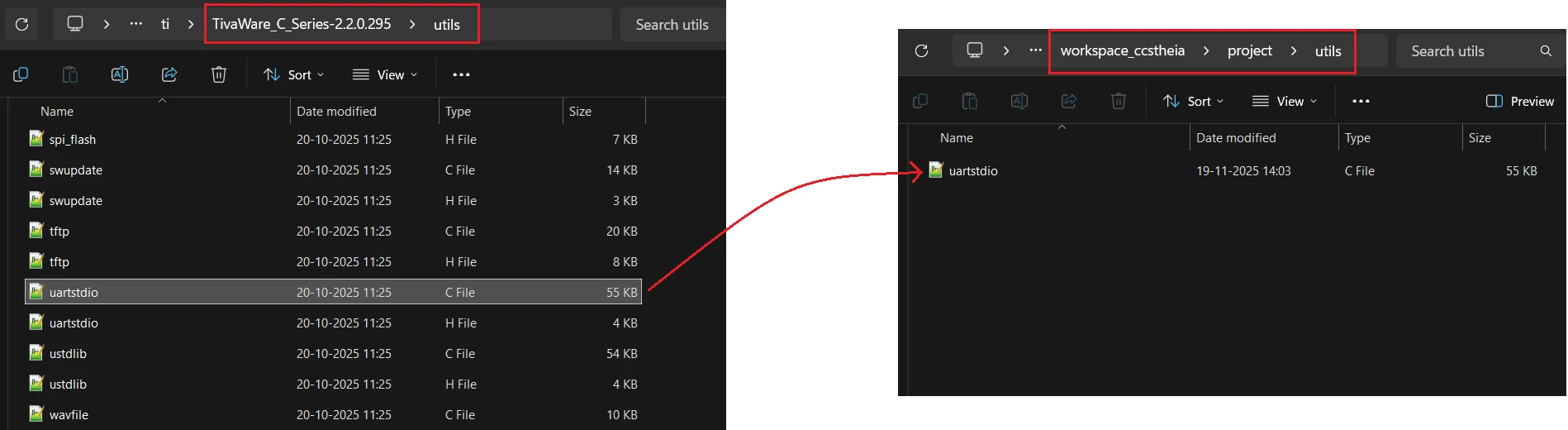
Required file: Copy uartstdio.c from your TivaWare installation (TivaWare/utils/uartstdio.c) into a utils/ folder inside your CCS project. Without it, the linker will report undefined references to UARTprintf and UARTStdioConfig.
Complete Main Code
int main(void)
{
    systemClockConfig();       // PLL: 80 MHz system clock
    IntMasterEnable();         // Enable global interrupts (required for SysTick delay)

    UART0_Init();
    SPI0_Init();

    UARTprintf("\n--- ADXL345 SPI Test ---\n");

    uint8_t id = ADXL345_ReadDeviceID();
    UARTprintf("Device ID = 0x%02X\n", id);

    while (1)
    {
    }
}The IntMasterEnable() call must come after all peripheral initialization to prevent interrupts from firing before the peripherals are ready. The Device ID is read once and printed; the infinite loop holds the MCU running so the output remains visible.
Serial Console Output
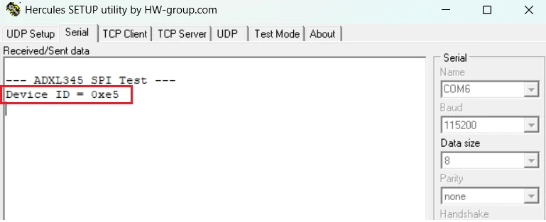
The terminal prints Device ID = 0xE5 — the expected fixed value from ADXL345 register 0x00. This single line confirms that SPI wiring, mode configuration, CS handling, and the read command format are all correct.
Logic Analyzer Output
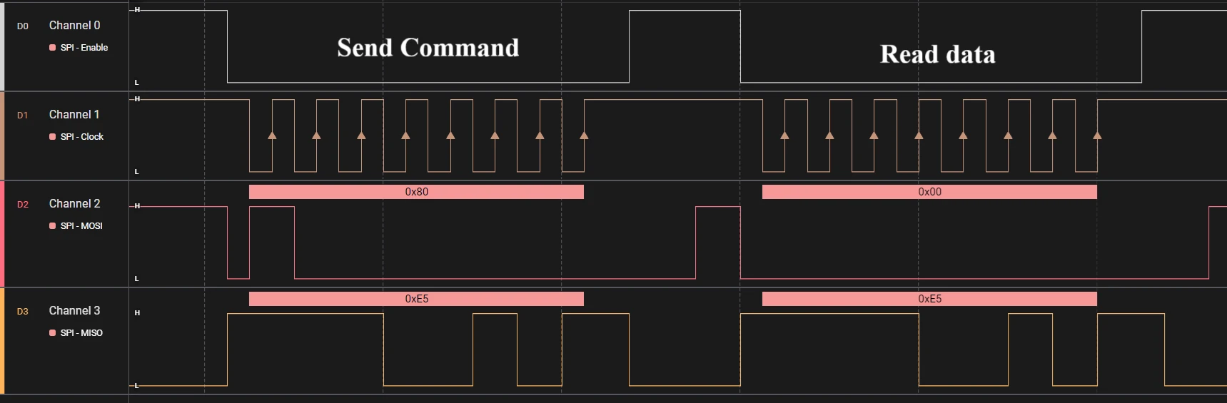
The logic analyzer capture shows the complete two-phase SPI read transaction. CS goes LOW to select the ADXL345. The master clocks out 0x80 on MOSI (register address 0x00 with read bit 7 set). On the following eight clock pulses, the master drives a dummy 0x00 while the ADXL345 returns 0xE5 on MISO. CS goes HIGH to end the transaction.
This timing diagram is worth bookmarking. The same pattern — CS low, command byte, dummy byte, read response, CS high — applies to virtually every SPI sensor and memory device you’ll encounter.
Troubleshooting SPI on TM4C123G
Getting 0x00? The CS line is not toggling correctly, or the register address is wrong. Add a UARTprintf() immediately after the GPIOPinWrite() CS-LOW call to confirm the code is actually reaching that point. Also verify GPIO_PIN_3 is not still configured as a UART or GPIO input pin — GPIOPinTypeSSI() must have been called on it.
Getting 0xFF? The MISO line is floating or disconnected. Check the physical connection between ADXL345 SDO and TM4C123G PA4. Confirm the ADXL345 is powered at 3.3 V with GND connected — an unpowered device cannot drive MISO.
Getting a random value? SPI mode is likely wrong. The ADXL345 requires Mode 3 — verify SSI_FRF_MOTO_MODE_3 is in your SSIConfigSetExpClk() call. If you previously called the function with a different mode and forgot to update it, the SSI module will retain the old mode until re-initialized.
Nothing on the logic analyzer? Peripheral clocks are probably not enabled. Confirm both SysCtlPeripheralEnable(SYSCTL_PERIPH_SSI0) and SysCtlPeripheralEnable(SYSCTL_PERIPH_GPIOA) are called before any GPIO pin configuration, and that the while (!SysCtlPeripheralReady(...)) loops have completed before you configure pins.
Intermittent or corrupt data? Power or ground issue — confirm the ADXL345 VCC is a steady 3.3 V and GND is shared with the TM4C123G. Loose jumper wires are the most common cause of intermittent SPI failures on bench setups. Reduce SPI speed to 1 MHz temporarily to rule out signal integrity problems.
TM4C123G SPI Frequently Asked Questions
Conclusion
A working Device ID = 0xE5 on your serial terminal means everything is correct: SSI0 is clocked and enabled, the GPIO pins are routed to their SPI alternate functions, Mode 3 timing matches the ADXL345's requirements, and CS is toggling at the right moments. That's a complete, verified SPI driver foundation — not just for the ADXL345, but for any SPI peripheral you connect to the TM4C123G going forward.
The read pattern used here — CS low, command byte with read bit, dummy byte to clock in the response, CS high — is the universal SPI register read idiom. The same SSIDataPut() / SSIBusy() / SSIDataGet() sequence works for multi-byte reads, writes, and burst transfers; you only change the command byte, the number of transfer cycles, and which register address you target.
From here, you can extend this driver to read ADXL345 axis data (registers 0x32–0x37), configure interrupt outputs, or port the same SPI init pattern to SSI1, SSI2, or SSI3 for multi-device setups. For the next steps in the TM4C123G series, see UART with Virtual COM Port, I2C with TivaWare, and the full TM4C123G Tutorial Index.
Download TM4C123G SPI Project Files
Complete CCS project with TivaWare source for SSI0 SPI init, ADXL345 Device ID read, and UART debug output. Includes basic_conf files, uartstdio.c, and main.c ready to build and flash. Free to download — support the work if it helped you.
Browse More TM4C123G Tutorials
TM4C123 Clock Configuration: Main Oscillator, PIOSC & PLL with TivaWare
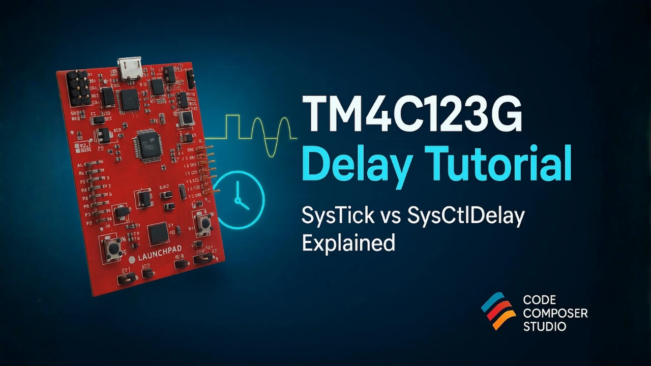
TM4C123G Delay Tutorial – Using SysCtlDelay and SysTick Timer

TM4C123 GPIO Tutorial – Digital Input and Output using Tiva C LaunchPad
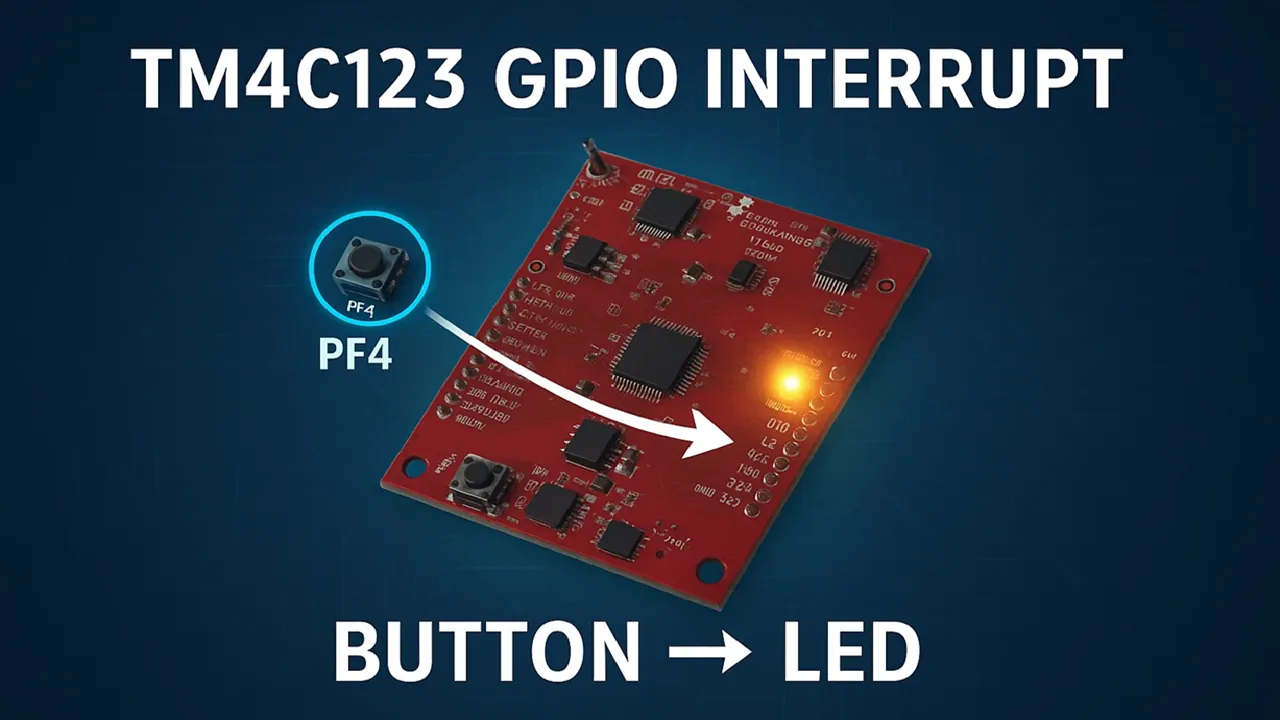
TM4C123 GPIO External Interrupts (Using TivaWare in Code Composer Studio)
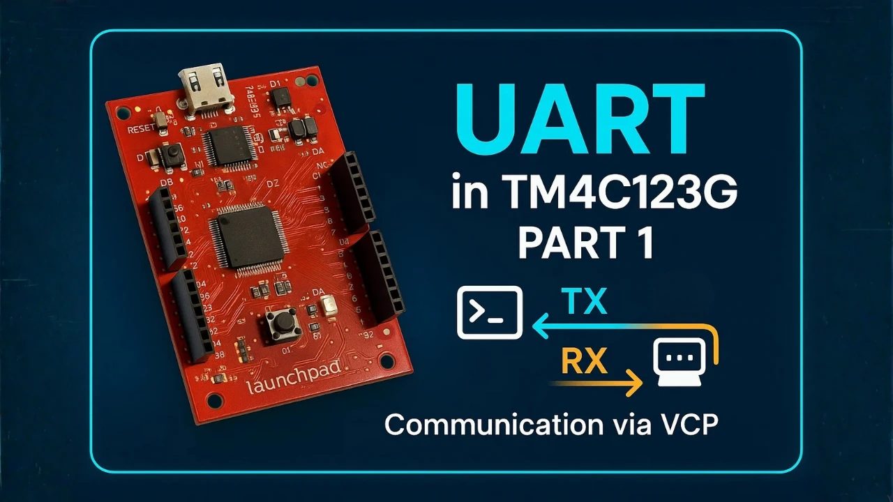
TM4C123G UART Tutorial (PART 1) – How to Use UART and Virtual COM Port in Tiva C

Subscribe
Login
0 Comments
Newest
