Last Updated: March 23, 2026
Learn how to cascade multiple MAX7219-based dot matrix displays with STM32 using SPI. Step-by-step wiring, cascading code, and column-to-row data conversion included. The project can be downloaded at the end of the post.
Recommended Resources:
This is the 2nd tutorial in a mini series covering the Dot Matrix Module with STM32 via SPI. In the previous tutorial we covered initialise the display and printing some characters on a single 8×8 dot matrix.
You should take a look at the previous tutorial before continuing with this one.
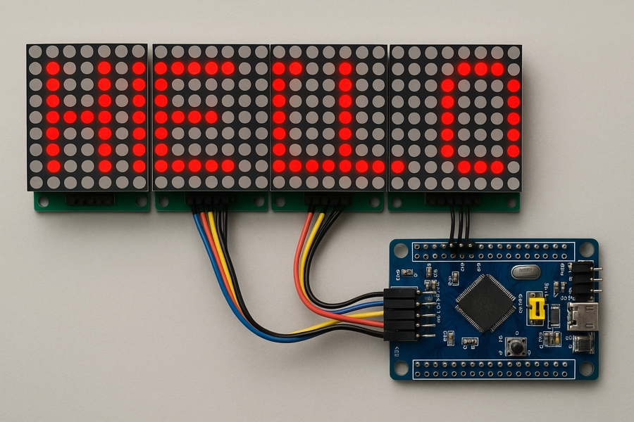
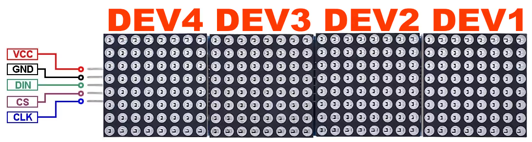
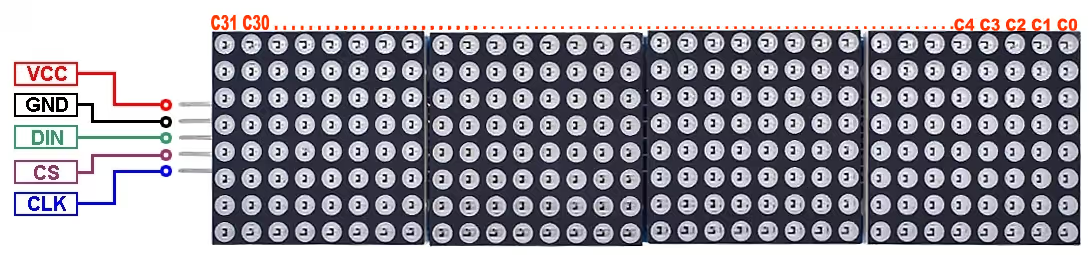
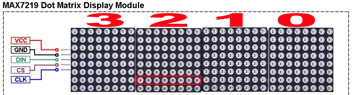
Today we will see how to cascade multiple dot matrix displays together. The device I am using has 4 dot matrix cascaded together and they all use the same pins. So we still have only 3 pins to connect to the MCU and using these 3 pins we will control 4 displays. Below is the image showing the device.
We will also see how to scroll characters and strings on these displays, but in the next part of this series. To scroll the characters on these displays, it is better to arrange our data in the column form. But if you remember the previous part of this series, the display I am using was accepting the data in the Row format. So today we will see how to convert the column data to the row format, so that our data in the column form can be printed on the displays.
VIDEO TUTORIAL
You can check the video to see the complete explanation and working of this project.
Introducing Dot Matrix Module
The dot matrix module with MAX7219 is a compact display unit that uses an 8×8 LED matrix controlled by the MAX7219 driver chip. It simplifies the process of controlling multiple LEDs by handling all the multiplexing and current regulation internally. Commonly used in electronics projects for scrolling text, symbols, or simple animations, it communicates with microcontrollers using the SPI protocol, making it efficient and easy to integrate with platforms like STM32, Arduino, and ESP32.
Some of the important features of Dot Matrix Module are:
- Built-in MAX7219 Driver:
Handles LED scanning, multiplexing, and current control, reducing microcontroller workload. - SPI Interface:
Communicates efficiently over a 3-wire SPI protocol (DIN, CLK, CS), supporting daisy chaining of multiple modules. - 8×8 LED Display:
Offers 64 individually addressable LEDs in a matrix format, ideal for characters and patterns. - Cascadable Design:
Multiple modules can be connected in series to create larger displays for scrolling text or graphics.
CUBEMX CONFIGURATION
Clock Configuration
Below is the image showing the clock configuration.
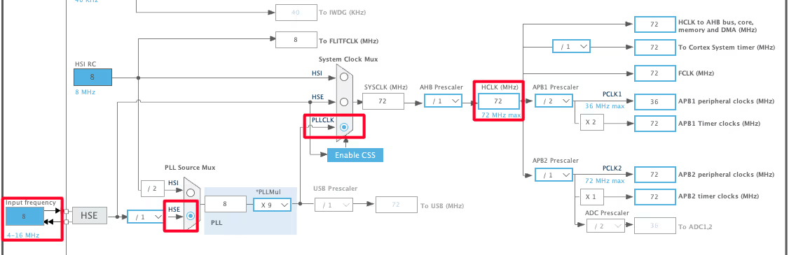
The STM32F103 is clocked by the external 8MHz crystal. The system is running at maximum 72MHz clock.
SPI Configuration
Below is the image showing the SPI configuration.
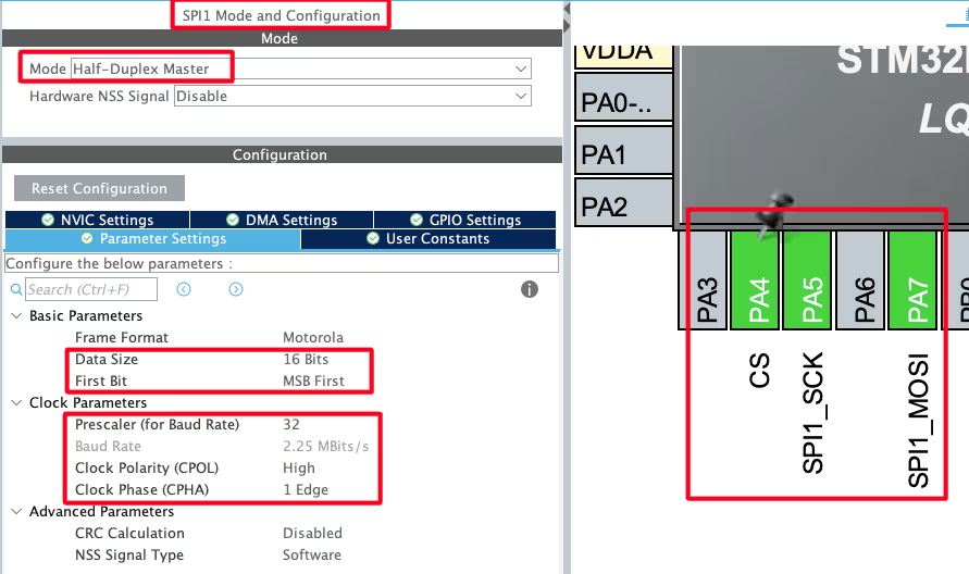
I am using the SPI1 for this tutorial. The SPI is configured in the Half Duplex Mode. This is because we only need the SPI to send the data to the display, but not receive anything from it.
- The Data Size is set to 16 bits with MSV first. This is because the MAX7219 expects the data in 16 bit format.
- There is no requirement for the Baud Rate, so I have configured it around 2 Mbps.
- The Clock Polarity is set to HIGH and Clock Phase is set to 1 Edge. This is important and as per the MAX7129 datasheet, the CPOL must be 1.
The pins PA5 and PA7 are configured as the SCK and MOSI pins. We will also set the pin PA4 as output and rename it to CS.
WIRING DIAGRAM
Below is the image showing the connection between STM32F103 and Dot Matrix Display.
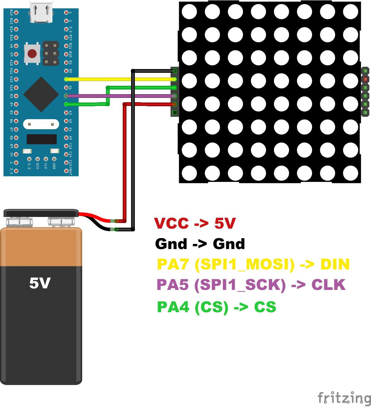
As you can see in the image above,
| STM32 Pin | SPI Function | Connected to Device Pin |
|---|---|---|
| PA5 | SPI1_SCK | CLK |
| PA7 | SPI1_MOSI | DIN |
| PA4 | CS | CS |
The device is powered with 5V supply from a battery. You must use some external power source for these type of displays. There are a lot of LEDs connected, and when they all are turned ON, they consume a lot of current. This might damage the MCU. Therefor use some external 5V power supply for these type of displays.
CASCADING THE DISPLAYS
When cascading the devices, connect all devices’ LOAD/CS inputs together and connect DOUT to DIN on adjacent devices. DOUT is a CMOS logic-level output that easily drives DIN of successively cascaded parts. If you purchase a display as shown above, it is already cascaded in this manner.
Sending Command
We need to send a few set of commands to initialise the display. We have already covered these commands in the previous tutorial, but they were sent to initialise a single device. Now we have multiple devices in the cascade, so each command needs to be sent as many times as the number of devices we have. This way the same command is latched to all the devices.
#define NUM_DEV 4

void max7219_cmd (uint8_t Addr, uint8_t data)
{
	uint16_t writeData = (Addr<<8)|data;
	HAL_GPIO_WritePin(CS_GPIO_Port, CS_Pin, 0);  // enable slave
	for (int i=0; i<NUM_DEV; i++)
	{
		HAL_SPI_Transmit(&hspi1, (uint8_t *)&writeData, 1, 100);
	}
	HAL_GPIO_WritePin(CS_GPIO_Port, CS_Pin, 1);  // disable slave
}The parameter of the function max7219_cmd are:
@Addr is the register address where we want to write the data
@data is the data byte itself.
- Inside this function, we will first combine both Register Address and the data byte in a single 16 bit variable.
- Then pull the CS pin LOW to enable the slave.
- Transmit the 16 bit data via the SPI to all the devices in the cascade. The function
HAL_SPI_Transmitexpects a pointer to the 8bit unsigned array, so we will typecast the address of the 16bit variable. - Pull the CS pin HIGH to disable the slave.
When the CS pin goes HIGH, the data word is latched in all the devices.
Initialisation
The Initialisation function remains the same as we used in the previous tutorial. Therefore I am not explaining it here.
void matrixInit (void)
{
	max7219_write(0x09, 0);  // no decoding
	max7219_write(0x0a, 0x01);  // 3/32 intensity
	max7219_write(0x0B, 0x07);  // scan all 7 columns
	max7219_write(0x0C, 0x01);  // normal operation
	max7219_write(0x0F, 0);     // No display test
}Sending Data
This is the part where we need to make a lot of changes. Below is the function to write the data to the device.
void max_write (int row, uint8_t data)
{
	int devTarget = (row - 1) / 8;  // find out which is the actual max, where we need to write the data
	int offset = devTarget * 8;  // The offset of the start byte for the devTarget in the buffer
uint16_t writeData = 0;The max_write function takes the following parameters:
- @row is the row number where we want to write the data. It can vary from 1 to 32 for the 4 devices in cascade.
- @data is the data byte that we want to write to the respective row.
Inside this function we will first determine the target device, devTarget. This is basically the device where the current row is located and where we will write the data to. For example, if the row number is 18, the devTarget will be (18-1)/8 = 2. This is considering that the device numbers starts from 0.
Next we will calculate the offset of the current row in the target device. The rows on each device ranges from 1 to 8, therefore we can not write data to any row number higher. than 8. If the current row is 18, it is actually the Row 2 in the device 2. The offset actually determines the start row number for the current device. For example, if the devTarget is 2, the offset will be 16. The row number for the current device start from 16 onwards.
Then we will define the 16 bit variable writeData. This variable will store the 4 bit row address and the 8 bit data byte altogether. We will send this 16 bit word to the device.
	HAL_GPIO_WritePin(CS_GPIO_Port, CS_Pin, 0);  // Select the slave
	for (int dev = 0; dev < NUM_DEV; dev++)   // for loop for all the max connected
	{
		if (dev == devTarget)  // if this the target
		{
			writeData = ((row - offset)<<8)|data;  // send the column number and the data byte
			HAL_SPI_Transmit(&hspi1, (uint8_t *)&writeData, 1, 1000);
}To send the data word to the display, we will first pull the CS pin low, so to select the device.
Since there are 4 devices cascaded together, we need to take extra care while sending the data. The data is sent in such a way that only the target device should receive the data, while the other devices should receive NO Operation command.
We will first call a for loop to cover all the connected devices. Inside this for loop, we will check if the the current device is the target device. If it is, then send the data word to the device.
The Row address is calculated by using row-offset. For example, if the row is 18 and the offset for the device 2 is 16, the row address will be 2.
So if the current device matches the target device, the data is sent to the given row. But for the rest of the devices, a. NO-Operation command is sent.
		else
		{
			writeData = 0;  // else send NOOP
			HAL_SPI_Transmit(&hspi1, (uint8_t *)&writeData, 1, 1000);
		}
	}
	HAL_GPIO_WritePin(CS_GPIO_Port, CS_Pin, 1);  // disable the slave
}The No-Operation command is explained in the image below.
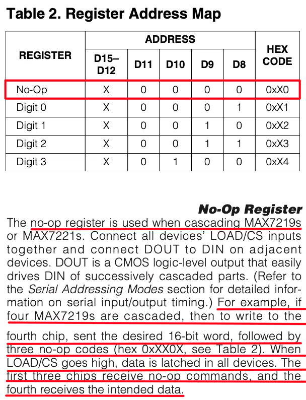
Basically, the No-Operation command is sent to the other devices, where we are not sending the data. This is exactly what we do in the max_write function.
One more thing to note here is that all the devices should receive the data or the No-Operation command while the CS pin is still Low. When the CS pin is pulled high, the respective data or command is latched to all the devices.
The main function
In the main function, we will simply initialise the display and send some random data to one of the devices.
int main ()
{
  ....
  matrixInit();
  max_write(17, 1);
  max_write(18, 2);
  max_write(19, 3);
  max_write(20, 4);
  max_write(21, 9);
  max_write(22, 12);
  while (1)
  {}
}Here We will write different data to different rows. The rows from 17 to 22 lies in the DEV 2, so we should see the data on this particular device only. The rest of the devices will receive the no operation command.
Below is the image showing the output of the above code.
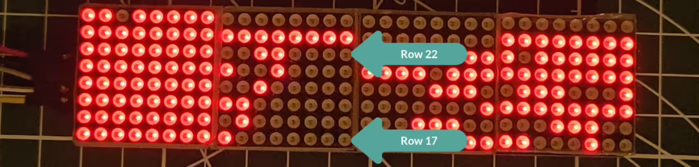
You can see the Rows 17 to 22 got updated with the data as per the code.
- The Row17 has the data 0x01.
- Row18 has the data 0x02.
- Similarly, the Row21 has the data 0x09 and Row22 has the data 0x0C.
ARRANGE DATA IN COLUMNS
We were able to successfully cascade the multiple devices. We also saw how to write the data on a particular device in the cascade. But the data was being written in terms of Rows. This is fine for displaying characters, but it would be harder to scroll the character or string in this format.
In the second half of this tutorial, we will see how to arrange the data in columns. This will make it easier for us to scroll the character or string on this display. The data will still be written in the form of the Rows as that is how the display accepts it, but we will just create another buffer to store this data in the form of columns.
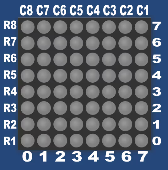
The column buffer is defined universally and it has 32 bytes to store the data for 32 columns.
#define NUM_DEV 4
uint8_t bufferCol[NUM_DEV*8];As I mentioned earlier, the data will be written in the Row form as this is how the device accepts it. So there will be no change in the way we send the data to the device. But we will define another function to convert the column data to the Row form, and then send it to the display.
void flushBuffer (void)
{
	uint8_t bufferRow[NUM_DEV*8] = {0};  // buffer to store data column wise

	/* Convert Cols to Rows */
	for (int i=0; i<NUM_DEV*8; i++)  // for loop for all the bytes
	{
		int dev = i/8;  // 0,1,2,3..  // keep track of which max is being written
		for (int j=0; j<8; j++)  // for loop to extract bits
		{
			if ((bufferCol[i])&(1<<(j)))  // if the bit is 1 // start extracting from the 0th bit of C0
			{
				bufferRow[j+(8*dev)] |= (1<<(7-(i-(8*dev))));  // start writing it from the 7th bit of R0
			}
		}
	}

	/* send Row Data */
	for (int row=1; row<=(NUM_DEV*8); row++)  // write the column data into the columns
	{
		max_write(row, bufferRow[row-1]);
	}
}The flushBuffer function perform 2 separate operations.
- It will first extract the data bits from column, and store them into the rows.
- It will then call the function
max_writeto send the converted row data to the device.
Inside this function, we will first define a Row buffer (bufferRow) to store the converted Row data. Then we will extract each bit from a particular column and store them into a particular position of each Row.
The variable i represents the column we are working on. It can vary from 0 to 31 (4 DEV). The variable dev will keep track of which device the current column is being selected for extraction.
The variable j represents the bit we are extracting from the current column. It will vary from 0 to 7. We will understand this entire setup using some examples.
When i=0
The dev = 0/8 = 0, this means that we are currently extracting the column of the first device.
When j=0, the statement bufferCol[i])&(1<<(j) will check the 0th bit in 0th column. If this bit is a 1, we will write a 1 to the 7th (1<<(7-(0-(0))) position of the 0th Row.
When j=7, the statement bufferCol[i])&(1<<(j) will check the 7th bit in 0th column. If this bit is a 1, we will write a 1 to the 7th (1<<(7-(0-(0))) position of the 7th Row.
This way all the bits from 0th Column will be extracted and the 7th bit of all the Rows will be modified according to it.
When i=4
The dev = 4/8 = 0, this means that we are currently extracting the column of the first device.
When j=0, the statement bufferCol[i])&(1<<(j) will check the 0th bit in 4th column. If this bit is a 1, we will write a 1 to the 3rd (1<<(7-(4-(0))) position of the 0th Row.
When j=7, the statement bufferCol[i])&(1<<(j) will check the 7th bit in 4th column. If this bit is a 1, we will write a 1 to the 3rd (1<<(7-(4-(0))) position of the 7th Row.
This way all the bits from 4th Column will be extracted and the 3rd bit of all the Rows will be modified according to it.
When i=10
The dev = 10/8 = 1, this means that we are currently extracting the column of the second device.
When j=0, the statement bufferCol[i])&(1<<(j) will check the 0th bit in 10th column. If this bit is a 1, we will write a 1 to the 5th (1<<(7-(10-(8))) position of the 0th Row of DEV1.
When j=7, the statement bufferCol[i])&(1<<(j) will check the 7th bit in 10th column. If this bit is a 1, we will write a 1 to the 5th (1<<(7-(10-(8))) position of the 7th Row of DEV1.
This way all the bits from 10th Column will be extracted and the 5th bit of all the Rows of DEV1 will be modified according to it.
The variable i will vary upto 31 and this way all the Rows of all the devices will be populated with the values extracted from the column buffer.
After storing the data in the rows, the data will be then sent to the devices.
	for (int row=1; row<=(NUM_DEV*8); row++)  // write the column data into the columns
	{
		max_write(row, bufferRow[row-1]);
}Here we will start sending the data, starting from row 1. Since the buffer starts from 0th element, we need to use row-1.
The main Function
We will configure the Dot Matrix Tool for the following configuration.
Column Major & Big Endian
Below is the output based on the configuration.
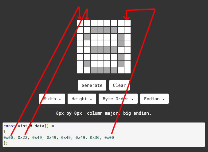
As you can see in the image above, the data in the output is arranged according to the columns. This is format in which we need the data. So we will copy this code to our main function.
Below is the main function.
const uint8_t data[] ={0x00, 0x22, 0x49, 0x49, 0x49, 0x49, 0x36, 0x00};

int main()
{
  ....
  matrixInit();
  clearDisplay();
  int indx=0;
  for (int i=5; i<13; i++)
  {
    bufferCol[i] = data[7-indx];
    indx++;
  }
  flushBuffer();
  while (1)
  {}
}We will copy the data, starting from the last byte, into the column buffer. Here I am storing the data, starting from the 5th column. This is to test if we are able to display a part of the number on both the adjacent devices.
After copying the data to the column buffer, we will call the function flushBuffer to flush the entire column buffer to the display.
Below is the image showing the output of the above code.
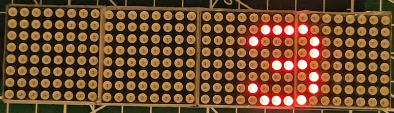
As you can see the number 3 is printed partly on both the devices. The data is able to cross the device boundary, and this is going to help us while scrolling the characters across this display.

Can you make tut on DWIN display
Stupid!!!
There is already a tut on DWIN. Please search it on the website.