Home ▸ STM32 Tutorials ▸ STM32 CAN ▸
Updated On: April 30, 2026
STM32 FDCAN Normal Mode: Configure Message RAM, Filters & Callbacks
The FDCAN Loopback tutorial got your peripheral working in self-test mode. Normal Mode is where FDCAN gets useful: two nodes on a real differential bus, transmitting and receiving through hardware filters, with the message RAM correctly partitioned between instances. The most common point of failure here — and what makes Normal Mode harder than Loopback — is the Message RAM. Get the offsets wrong and both peripherals corrupt each other’s data silently.
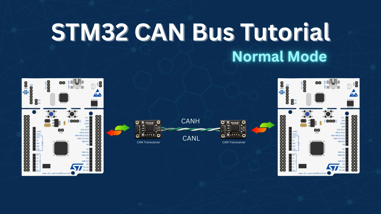
This tutorial demonstrates STM32 FDCAN Normal Mode using the STM32H745 Discovery board, which has two built-in FDCAN peripherals and an onboard MCP2562FDT transceiver. You will configure FDCAN1 and FDCAN2 to communicate with each other over the onboard CANH/CANL bus — no external CAN device needed. The tutorial covers Message RAM partitioning for dual instances, bit timing using the Kvaser calculator, ID mask filter setup for FIFO0 and FIFO1, and the complete TX/RX callback pattern using HAL_FDCAN_AddMessageToTxFifoQ, HAL_FDCAN_ActivateNotification, and HAL_FDCAN_GetRxMessage.
This is Part 3 of the STM32 CAN Bus series. You can check the other tutorials of this series below:
STM32 FDCAN: How It Works
What is FDCAN and Why Use It?
FDCAN, or Flexible Data-Rate Controller Area Network, is a communication protocol that lets microcontrollers talk to each other quickly and reliably. Unlike standard CAN, FDCAN supports higher data speeds and flexible message sizes. STM32 microcontrollers use FDCAN to connect with sensors, motors, and other devices in automotive, industrial, and robotics projects. You use FDCAN when you need fast, stable, and error-free communication between multiple devices.
Key Features of FDCAN in STM32
STM32 microcontrollers come with a built-in FDCAN controller that makes setup and communication easier. Some key features include:
- Flexible Data Rate: Supports both standard and fast data speeds.
- Error Detection: Built-in error checking keeps your communication reliable.
- Multiple Message Objects: Handles many messages at the same time.
- Low Latency: Quick data transmission with minimal delay.
- Filter Options: Lets you receive only the messages you need.
These features make STM32 FDCAN perfect for real-time communication in complex systems.
Normal Mode vs Loopback, Silent & Restricted
FDCAN supports several operating modes, each designed for a specific purpose. Normal Mode is the standard mode where the node actively participates in the network: it can send and receive messages, acknowledge frames, and detect errors.
Other modes include:
- Loopback Mode: The node only tests its own transmission without sending data on the bus.
- Silent Mode: The node listens to messages but does not transmit or acknowledge.
- Restricted Mode: Combines features like silent and limited communication for diagnostics.
Unlike these special modes, Normal Mode enables full communication, making it suitable for real-time network operation.
Use Normal Mode when your STM32 is part of an active CAN or CAN-FD network and needs to:
- Transmit messages to other nodes.
- Receive messages from sensors, controllers, or actuators.
- Detect and report errors on the bus.
Normal Mode is the default operating mode for most real-world applications where continuous communication is required.
CAN 2.0 vs CAN-FD: Frame Structure Comparison
Below is an illustration showing the structure of an FDCAN frame:
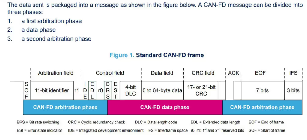
The FDCAN frame is divided into three main phases:
- First Arbitration Phase
This phase identifies the message and its purpose:- Start of Frame (SOF): Marks the beginning of the message.
- ID and Control Bits: Include the message ID, indicate whether data is being sent or requested, and specify the protocol type (CAN or CAN-FD) and speed configuration.
- Data Transmission Phase
Here the actual information is sent:- Data Length Code (DLC): Shows how many bytes of data are included.
- Data: The actual message content you want to transmit.
- Cyclic Redundancy Check (CRC): Verifies data integrity.
- Dominant Bit: Signals control for proper timing and synchronization.
- Second Arbitration Phase
This phase confirms successful message delivery:- Acknowledgment (ACK): Sent by receivers to confirm the message was received.
- End of Frame (EOF): Marks the end of the message.
During the Interframe Space (IFS), no data is transmitted. This pause separates one frame from the next.
CAN 2.0 vs CAN-FD
Let’s compare how CAN 2.0 and CAN-FD frames differ:
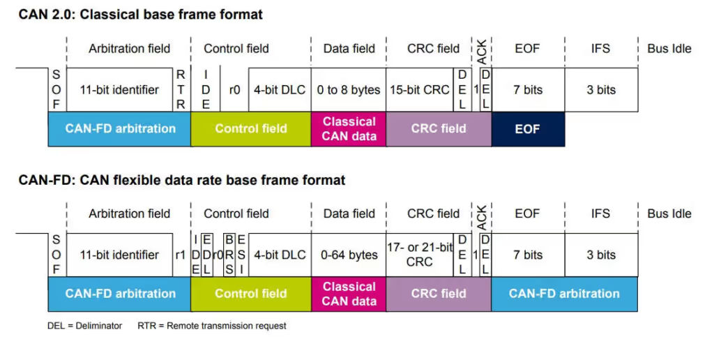
- Frame Type:
- CAN 2.0 uses the RTR bit to indicate a data frame (dominant) or a remote frame (recessive).
- CAN-FD always uses a dominant reserved (RRS) bit since it supports only data frames.
- New Control Bits in CAN-FD:
- EDL (Extended Data Length): Recessive to indicate a CAN-FD frame; in CAN 2.0, this bit is called R0.
- BRS (Bit Rate Switching): Indicates if a higher bit rate is used during the data phase.
- ESI (Error State Indicator): Shows whether the node is in an error-active or error-passive state.
Here’s a visual summary of the key differences:
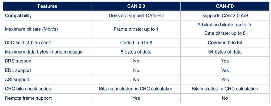
- CAN-FD supports larger payloads and faster data rates.
- It has additional control bits for flexibility, error detection, and speed switching.
- CAN 2.0 is simpler, supporting only fixed data length and a single bit rate.
STM32 FDCAN Wiring & CubeMX Setup
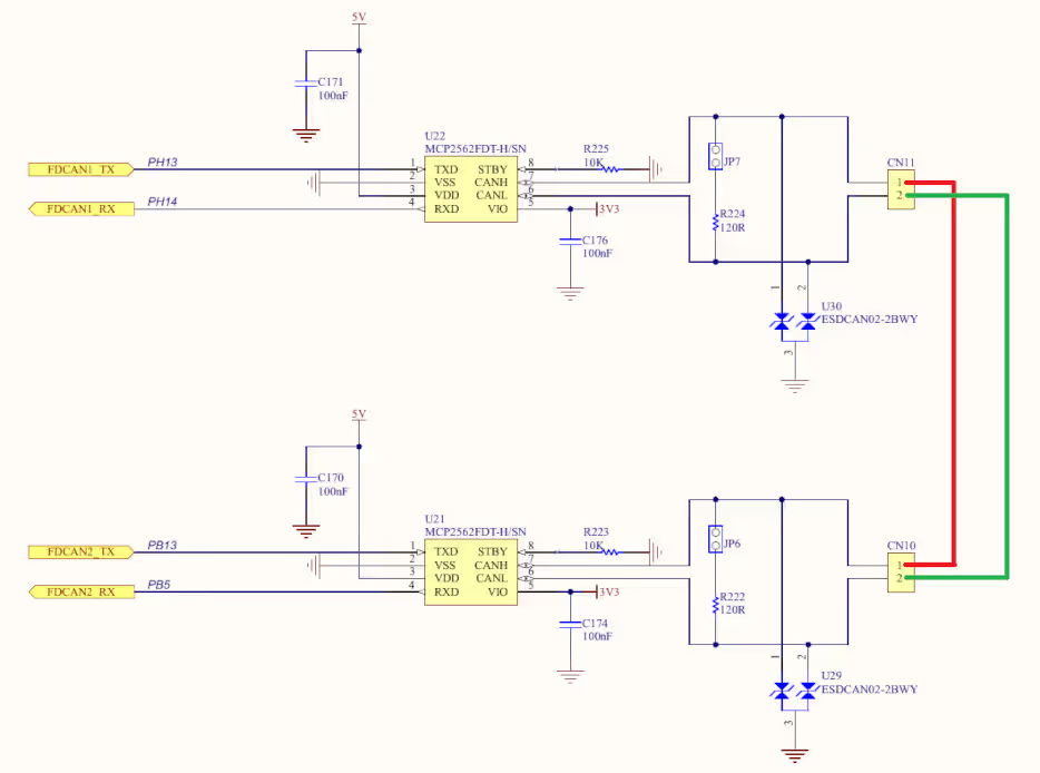
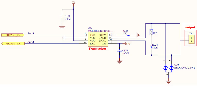
Hardware: STM32H745 Discovery with Onboard Transceivers
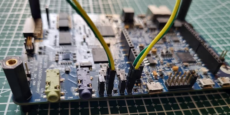
As mentioned earlier, I will use both FDCAN peripherals on the same STM32 board. Since the board already has two built-in transceivers, all we need to do is connect CANH to CANH and CANL to CANL.
Below is an image showing the exact connections:
Clock Configuration
Let’s start by configuring the clock first.
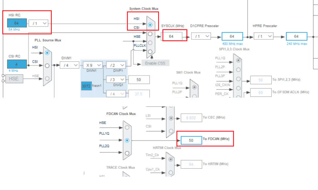
I am choosing the 64 MHz internal clock in this tutorial. The reason for the same will be explained in a while. Also note that the FDCAN clock is 50 MHz. This will be used in the later part of the tutorial.
Enabling FDCAN1 and FDCAN2 in CubeMX
Now enable the FDCAN peripherals for the cortex M7.
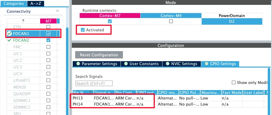
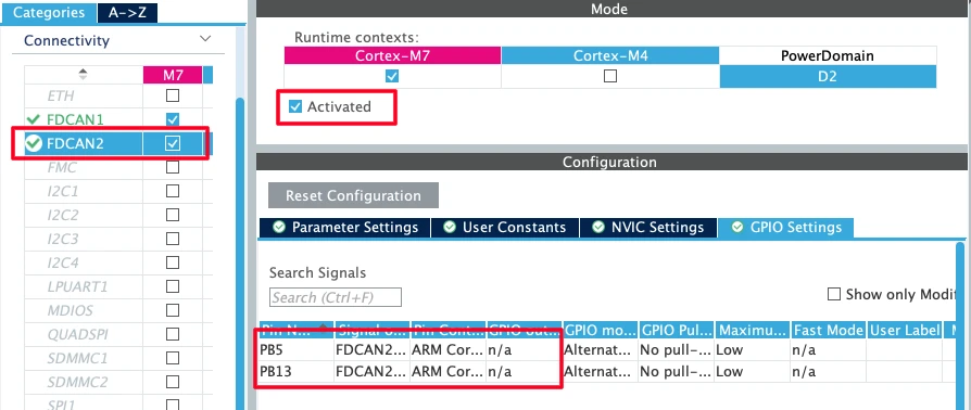
Here I have enabled the FDCAN1 and FDCAN2 for the cortex M7. Note the pins PH13 is the TX pin and PH14 is the RX pin in FDCAN1 and similarly PB5 and PB13 are the pins used for FDCAN2.
The controller I’m using, STM32H745 Discovery, has a built-in CAN transceiver on the board. The MCP2562FDT transceiver connects to pins PH13 (CANH) and PH14 (CANL). The board provides dedicated connectors for CANH and CANL, as shown in the image below:
Bit Timing Configuration (Using the Kvaser Calculator)
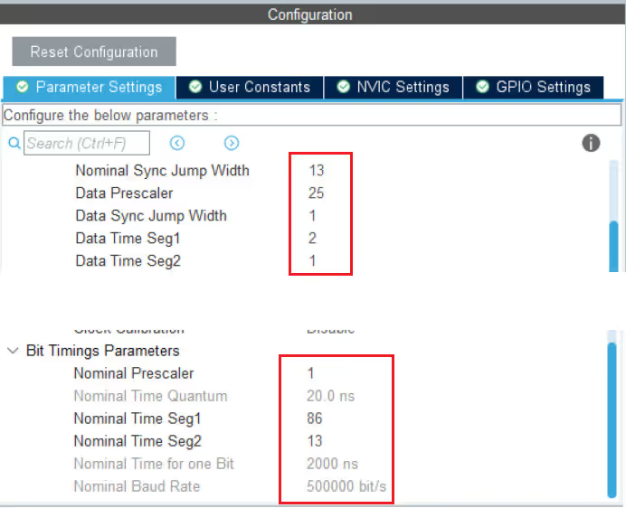
First we will take a look at the common configuration for both FDCAN1 and FDCAN2. This part includes Sync jump width, Prescaler, Time segment etc. In order to achieve the same board rate, both the peripherals must be configured similarly.
The image below shows the CAN-FD Parameter settings.
To calculate these set of parameters we need to use an external calculator, which could be found at https://www.kvaser.com/support/calculators/can-fd-bit-timing-calculator/
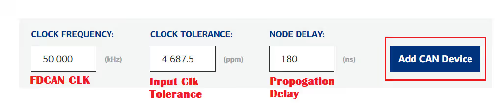
The first 3 parameters we need to input are the FDCAN CLK Frequency, The Input CLK Tolerance and the Transceiver node delay.
- The FDCAN clock Frequency is 50 MHz and we have already covered this in the clock configuration section.
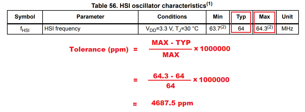
- Next comes the Clock Tolerance. I mentioned in the beginning that I am using the internal clock in this tutorial, and it was because it’s easier to find the clock tolerance for the input clock. The picture below is from the datasheet of STM32H745, showing the characteristics of HSI oscillator.
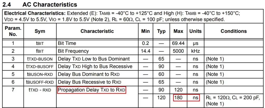
- Finally we have the node delay or Propagation Delay. This can be found in the AC characteristics of the Transceiver you are using. The image below shows the same for MCP2562FD, CAN-FD transceiver used in STM32H7 discovery.
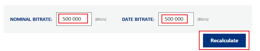
Next we have to input the bitrates that we want to set for the CAN-FD. As I already mentioned the FDCAN can transfer arbitration field and data filed at different bitrates. But I want to use the same bitrate for both of them, and that would be 500 Kbps. After you have entered the bitrates, click recalculate to calculate the values.
After we click the recalculate button, we will get the values of the parameters. This is shown in the picture below
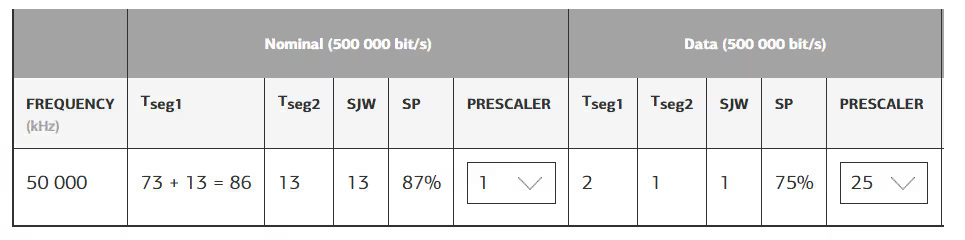
We can input these values in the FDCAN parameters. You should use the same values in both FDCAN instances.

Message RAM Configuration (Common Settings)
Now we will see the rest of the parameters. The arrows shows the parameters which has been modified.
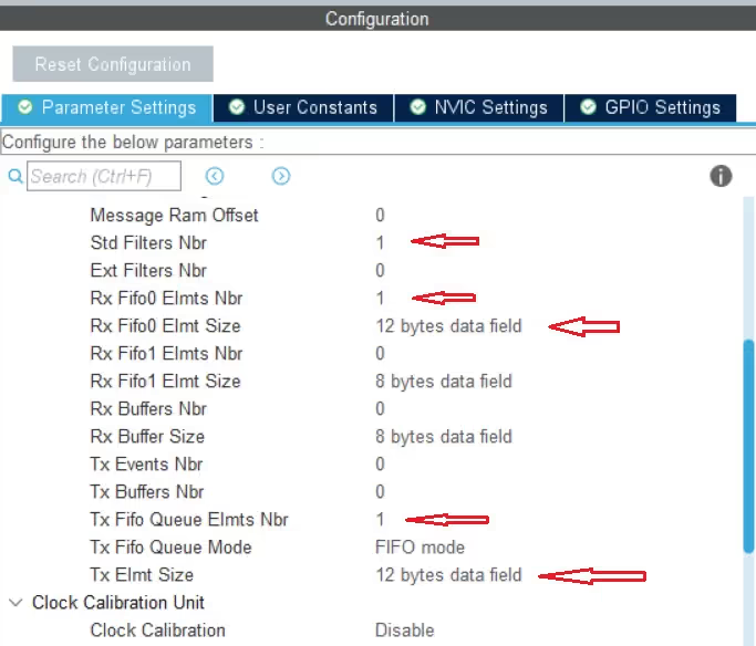
- In the image above, the message Ram offset is set to 0. This is used in the multiple instances of the FDCAN and will be covered later in the tutorial.
Std Filters Nbris the number of standard (ID) filters we are using.- We can use up to 128 different filters configured to accept or reject messages from different IDs
- I am only using a single filter.
Ext Filters Nbris set to 0 because we are not using any Extended IDs in this tutorial- We will use the RX FIFO 0 to receive the message. Totally we can use up to 64 FIFO elements and each element can store up to 64 bytes of data.
- Here I am only using a single element to receive 12 bytes of data.
- I am not using any RX buffer or TX buffer, so all those parameters are set to 0.
- TX Fifo will be used to send the data to the CAN bus. So here I am using 1 element of the TX Fifo to send 12 bytes of data.
Message RAM Partitioning (FDCAN1 and FDCAN2)
So far we covered the common configuration needed for both the instances. Since we want the 2 instances to act as 2 separate devices, we need to configure them separately.
Below are the configurations for FDCAN1 and FDCAN2.
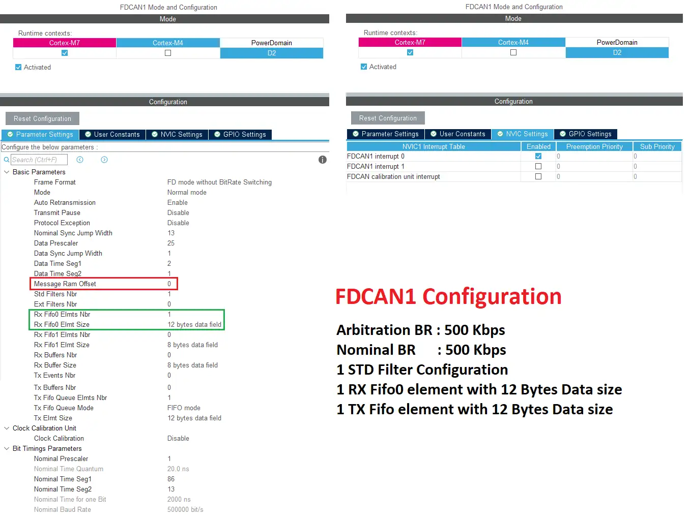

Other than the message RAM, one more change you can notice is that I am using the RX Fifo 0 for the FDCAN1, and RX Fifo 1 for the FDCAN2. This is simply because the 2 Fifos are available and I want to write completely separate codes for them.
Note that the message RAM offset for the FDCAN1 is 0, and that of the FDCAN2 is 11 words.
Why Message RAM Partitioning Matters in STM32 FDCAN
When using more than one STM32 FDCAN peripheral, correct message RAM partitioning is critical.
- STM32H7 provides 2560 words (~10 KB) of message RAM.
- You must allocate offsets for each FDCAN instance (e.g., FDCAN1 at offset 0, FDCAN2 at 11 words).
- Each filter, RX FIFO, and TX buffer consumes message RAM depending on data length.
As per the application note AN5348, the FDCAN message RAM is 2560 words in size, which is equivalent to 10KB. This RAM is provided to store the different filters, RX buffers/FIFOs, the TX buffers etc.
Understanding the FDCAN Message RAM Map
If we are using more than 1 FDCAN instance, we have to carefully partition the RAM such that the total size of these sections do not exceed the ram size. Below is the image shown as per the application note.
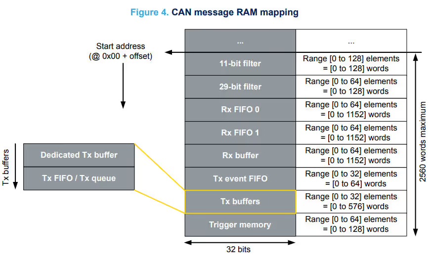
Note that different sections have different number of elements available. These elements are basically the number of these sections we can use. For eg- There are 128 elements available in the standard filter (11 bit filter), so we can use 128 different standard filters.
Similarly there are 128 elements in the RX buffer, so we can use 128 different buffers to receive data, and each buffer is capable of storing upto 64 bytes of data.
How much if the space will be occupied by each element of these sections is shown in the picture below.
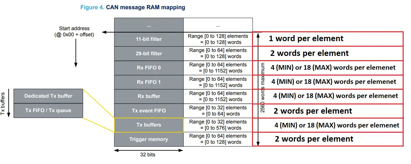
For most of the sections, the calculation here is pretty simple, (number of words available / number of elements). Though this rule does not apply in case of TX and RX buffers/Fifos. For these sections, the occupied space also depends on the data size we are using.
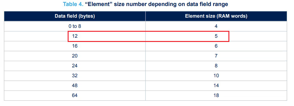
In the FDCAN1 configuration I have set the message Ram offset to 0, so the allocation will start at the beginning of the RAM.
I am using 1 standard filter (1 word) + 1 RX Fifo element with 12 bytes of data (5 words) + 1 TX Fifo element with 12 bytes of data (5 words). This totally makes 11 words.
These 11 words will be needed by the FDCAN1 to work properly, so the offset for the FDCAN2 is set to 11. The rest of the RAM is available to the FDCAN2, though it will also use 11 words.

STM32 FDCAN Code, Filters & Results
Filters in FDCAN allow your STM32 to selectively receive messages from the network. By configuring filters, you can decide which message IDs your node should process and which ones to ignore. Proper filter setup improves bus efficiency and reduces unnecessary processing, especially on busy networks. In this section, we’ll look at how to configure FDCAN filters step by step, so your application only handles the messages it needs.
Filter Configuration: FDCAN1 (FIFO0, ID 0x22)
FDCAN_FilterTypeDef sFilterConfig;

sFilterConfig.IdType = FDCAN_STANDARD_ID;
sFilterConfig.FilterIndex = 0;
sFilterConfig.FilterType = FDCAN_FILTER_MASK;
sFilterConfig.FilterConfig = FDCAN_FILTER_TO_RXFIFO0;
sFilterConfig.FilterID1 = 0x22;
sFilterConfig.FilterID2 = 0x22;
sFilterConfig.RxBufferIndex = 0;
if (HAL_FDCAN_ConfigFilter(&hfdcan1, &sFilterConfig) != HAL_OK)
{
  /* Filter configuration Error */
  Error_Handler();
}- The IdType defines if we are using the Standard IDs or Extended IDs
- Filterindex is used in case of configuring the multiple filters. Since I am only using 1 filter, it is set to 0.
- FilterType is the type of filter we are using. Here I am using the MASK Filter.
- For this MASK Filter, the ID1 (0x22) will act as the ID and ID2 (0x22) will act as the mask bits.
- If you want to learn more about how this works, I would suggest that you watch https://youtu.be/JfWlIY0zAIc
- FilterConfig decides what should be done to the messages that pass through the filter. It is set to be sent to RX FIFO 0.
- RxBufferIndex is used if you use the RX Buffer instead of FIFO, so it is set 0 her.
So all the messages coming from the ID 0x22 will be passed through the filter and get stored in the RXFIFO0.
Filter Configuration: FDCAN2 (FIFO1, ID 0x11)
FDCAN_FilterTypeDef sFilterConfig;

sFilterConfig.IdType = FDCAN_STANDARD_ID;
sFilterConfig.FilterIndex = 0;
sFilterConfig.FilterType = FDCAN_FILTER_MASK;
sFilterConfig.FilterConfig = FDCAN_FILTER_TO_RXFIFO1;
sFilterConfig.FilterID1 = 0x11;
sFilterConfig.FilterID2 = 0x11;
sFilterConfig.RxBufferIndex = 0;
if (HAL_FDCAN_ConfigFilter(&hfdcan2, &sFilterConfig) != HAL_OK)
{
  /* Filter configuration Error */
  Error_Handler();
}Here everything is similar except the ID is set to 0x11, and we are using RXFIFO1.
So all the messages coming from the ID 0x11 will be passed through the filter and get stored in the RXFIFO1.
Key HAL FDCAN Functions
Many searches are for STM32 HAL functions directly. Here’s what they do:
HAL_FDCAN_AddMessageToTxFifoQ→ Queues data for transmission.HAL_FDCAN_ActivateNotification→ Enables interrupts for RX FIFO events.HAL_FDCAN_GetRxMessage→ Retrieves incoming messages from RX FIFO.HAL_FDCAN_ConfigFilter→ Defines filter IDs and routing.HAL_FDCAN_RxFifo0Callback / HAL_FDCAN_RxFifo1Callback→ Called when new messages arrive.
Let’s dive into the implementation. The following code initializes the FDCAN peripheral, configures the message RAM, and sets up filters to handle incoming messages.
Variable Definitions
Below are the definitions we will use in this project.
// FDCAN1 Defines
FDCAN_TxHeaderTypeDef   TxHeader1;
FDCAN_RxHeaderTypeDef   RxHeader1;
uint8_t               TxData1[12];
uint8_t               RxData1[12];


// FDCAN2 Defines
FDCAN_TxHeaderTypeDef   TxHeader2;
FDCAN_RxHeaderTypeDef   RxHeader2;
uint8_t               TxData2[12];
uint8_t RxData2[12];As shown above, the RX and TX headers are defined separately for both the FDCANs. Also the RxData and TxData arrays are 12 bytes in size.
Starting FDCAN and Activating Notifications
We will write the start process for the FDCAN Peripheral inside the main function.
// STart FDCAN1
if(HAL_FDCAN_Start(&hfdcan1)!= HAL_OK)
{
 Error_Handler();
}

// STart FDCAN2
if(HAL_FDCAN_Start(&hfdcan2)!= HAL_OK)
{
 Error_Handler();
}

// Activate the notification for new data in FIFO0 for FDCAN1
if (HAL_FDCAN_ActivateNotification(&hfdcan1, FDCAN_IT_RX_FIFO0_NEW_MESSAGE, 0) != HAL_OK)
{
  /* Notification Error */
  Error_Handler();
}


// Activate the notification for new data in FIFO1 for FDCAN2
if (HAL_FDCAN_ActivateNotification(&hfdcan2, FDCAN_IT_RX_FIFO1_NEW_MESSAGE, 0) != HAL_OK)
{
  /* Notification Error */
  Error_Handler();
}First of all Start both FDCAN1 and FDCAN2. Then Activate the notification for new message to arrive in their respective Fifos. This notification will trigger the interrupt, which will eventually call a callback function, and there we will handle the incoming data.
TX Header Configuration (FDCAN1 and FDCAN2)
Next, prepare the TX header for both FDCAN, which will be transmitted along with the data on the can bus.. This header will remain the same and we can modify the data part later on the requirement. I am using maximum 12 bytes for data, hence it can also be declared in the beginning itself.
// Configure TX Header for FDCAN1
TxHeader1.Identifier = 0x11;
TxHeader1.IdType = FDCAN_STANDARD_ID;
TxHeader1.TxFrameType = FDCAN_DATA_FRAME;
TxHeader1.DataLength = FDCAN_DLC_BYTES_12;
TxHeader1.ErrorStateIndicator = FDCAN_ESI_ACTIVE;
TxHeader1.BitRateSwitch = FDCAN_BRS_OFF;
TxHeader1.FDFormat = FDCAN_FD_CAN;
TxHeader1.TxEventFifoControl = FDCAN_NO_TX_EVENTS;
TxHeader1.MessageMarker = 0;


// Configure TX Header for FDCAN2
TxHeader2.Identifier = 0x22;
TxHeader2.IdType = FDCAN_STANDARD_ID;
TxHeader2.TxFrameType = FDCAN_DATA_FRAME;
TxHeader2.DataLength = FDCAN_DLC_BYTES_12;
TxHeader2.ErrorStateIndicator = FDCAN_ESI_ACTIVE;
TxHeader2.BitRateSwitch = FDCAN_BRS_OFF;
TxHeader2.FDFormat = FDCAN_FD_CAN;
TxHeader2.TxEventFifoControl = FDCAN_NO_TX_EVENTS;
TxHeader2.MessageMarker = 0;The ID of the FDCAN1 is set to 0x11, and that of the FDCAN2 is set to 0x22. The rest of the parameters are same in both cases.
- The Identifier is the ID of the Transmitter, which is going to be 0x11 for the FDCAN1 and 0x22 for the FDCAN2.
- The IdType is set to Standard ID as we are not using Extended ID in this tutorial.
- TxFrameType implies whether we are sending a Data frame or Remote frame. It is set to Data Frame.
- DataLength is set to 12 bytes. This is the length of the actual Data we are going to send.
- ErrorStateIndicator is active and it will notify us if there is any error in transmission.
- BitrateSwitch is OFF, as I mentioned we will be using the same bitrate for both Arbitration and Data Fields
- FDFormat implies whether you want to use the standard CAN or FD CAN. It is set to FD_CAN
- We are not using the TxEvent or MessageMarker.
Main Loop: FDCAN1 Transmit Every 1 Second
Inside the while loop, we will make the the FDCAN1 to transmit the data every 1 second.
while (1)
{
 sprintf ((char *)TxData1, "FDCAN1TX %d", indx++);

 if (HAL_FDCAN_AddMessageToTxFifoQ(&hfdcan1, &TxHeader1, TxData1)!= HAL_OK)
 {
  Error_Handler();
 }
 HAL_Delay (1000);
}- The TxData contains a string (To indicate the data is coming from the FDCAN1) along with the incremented value of the indx variable.
- Then the function
HAL_FDCAN_AddMessageToTxFifoQwill add the message to the FIFO queue. - After the message is added to the FIFO Queue, it will be transferred to the CAN Bus
Once the message has been sent to the can bus, it will be received by all the devices that are attached to this bus (though we have only 1 more). And after the message passes through the filter of the FDCAN2, the new message callback will be called.
FDCAN2 RxFifo1 Callback: Receive and Respond
Since the FDCAN1 transmits the data in the while loop, the FDCAN2 will receive this data. Once the data is passed through the FDCAN2 filters, an interrupt will trigger and the HAL_FDCAN_RxFifo1Callback will be called. We will handle the data received inside this callback.
// FDCAN2 Callback
void HAL_FDCAN_RxFifo1Callback(FDCAN_HandleTypeDef *hfdcan, uint32_t RxFifo1ITs)
{
  if((RxFifo1ITs & FDCAN_IT_RX_FIFO1_NEW_MESSAGE) != RESET)
  {
    /* Retreive Rx messages from RX FIFO1 */
    if (HAL_FDCAN_GetRxMessage(hfdcan, FDCAN_RX_FIFO1, &RxHeader2, RxData2) != HAL_OK)
    {
    /* Reception Error */
    Error_Handler();
    }

    if (HAL_FDCAN_ActivateNotification(hfdcan, FDCAN_IT_RX_FIFO1_NEW_MESSAGE, 0) != HAL_OK)
    {
      /* Notification Error */
      Error_Handler();
    }

	  sprintf ((char *)TxData2, "FDCAN2TX %d", indx++);

	  if (HAL_FDCAN_AddMessageToTxFifoQ(&hfdcan2, &TxHeader2, TxData2)!= HAL_OK)
	  {
		  Error_Handler();
	  }
  }
}The RxFifo1Callback will be triggered since we are using the Fifo1 for the FDCAN2.
- Here we will first copy the Header information from the RX FIFO1 into the RxHeader, and data into the RxData array.
- We will then activate the notification for the new message again.
- At last we will send some data on the CAN bus.
- This data contains the string (To indicate the data is coming from the FDCAN2) along with the incremented value of the indx variable.
Once the message has been sent to the can bus, it will pass through the filter of the FDCAN1 and the new message callback will be called.
FDCAN1 RxFifo0 Callback: Receive and Re-arm
After receiving data from FDCAN1, the FDCAN2 processes this data and send something back to the CAN Bus. Once the data is passed through the FDCAN1 filters, an interrupt will trigger and the HAL_FDCAN_RxFifo0Callback will be called. We will handle the data received inside this callback.
// FDCAN1 Callback
void HAL_FDCAN_RxFifo0Callback(FDCAN_HandleTypeDef *hfdcan, uint32_t RxFifo0ITs)
{
  if((RxFifo0ITs & FDCAN_IT_RX_FIFO0_NEW_MESSAGE) != RESET)
  {
    /* Retreive Rx messages from RX FIFO0 */
    if (HAL_FDCAN_GetRxMessage(hfdcan, FDCAN_RX_FIFO0, &RxHeader1, RxData1) != HAL_OK)
    {
    /* Reception Error */
    Error_Handler();
    }

    if (HAL_FDCAN_ActivateNotification(hfdcan, FDCAN_IT_RX_FIFO0_NEW_MESSAGE, 0) != HAL_OK)
    {
      /* Notification Error */
      Error_Handler();
    }
  }
}The RxFifo0Callback will be triggered since we are using the Fifo0 for the FDCAN1.
- Here we will first copy the Header information from the RX FIFO0 into the RxHeader, and data into the RxData array.
- We will then activate the notification for the new message again.
Unlike the FDCAN2 callback, we are not transmitting any data here, since the data is being transmitted every second by the FDCAN1 in the while loop. This way the FDCAN1 will keep transmitting every 1 second, and FDCAN2 will always send a response to that.
Communication Results: FDCAN1 ↔ FDCAN2 Verified
The images below shows the data transmitted by one instance and received by another instance of the FDCAN in STM32.
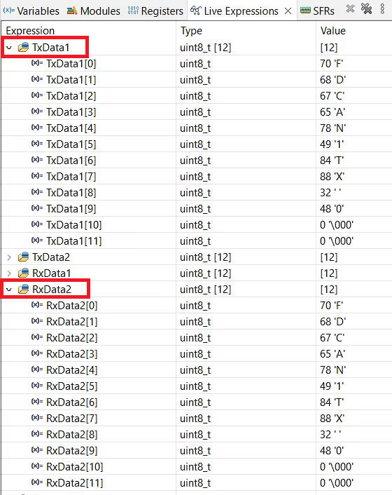
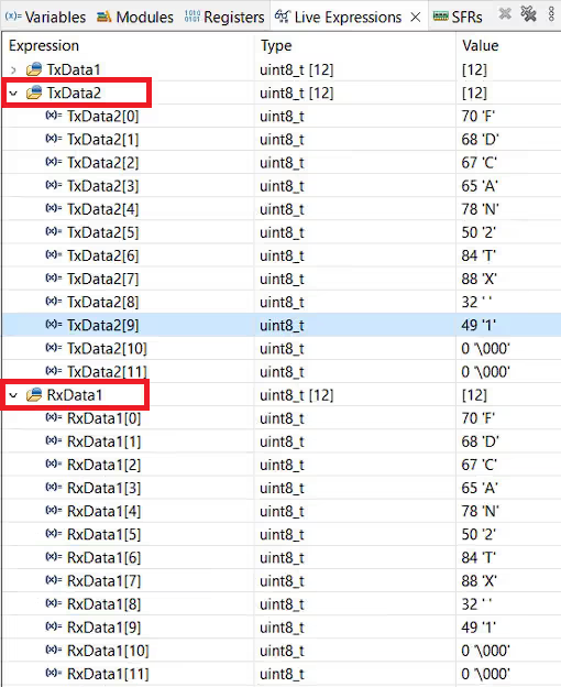
The first picture shows the data transmitted by FDCAN1 (TxData1) and the same data being successfully received by FDCAN2 (RxData2). The second picture shows a different data set transmitted by FDCAN2 (TxData2) and correctly received by FDCAN1 (RxData1).
This demonstrates that both FDCAN peripherals are communicating correctly, confirming that the transmission and reception setup is working in normal mode. It also verifies that the CANH and CANL connections are properly configured, and the data integrity is maintained across the network.
This test is important because it confirms reliable two-way communication between the nodes, which is essential in real-world applications like automotive systems, industrial automation, and robotics, where data must be accurately transmitted and received without errors.
STM32 FDCAN Normal Mode: Message RAM, Filters & HAL — Video Tutorial
This video walks through the complete STM32 FDCAN Normal Mode setup on the STM32H745 Discovery — clock configuration, enabling FDCAN1 and FDCAN2 in CubeMX, calculating bit timing with the Kvaser tool, partitioning the 2560-word Message RAM between two instances, configuring ID mask filters for FIFO0 and FIFO1, and writing the complete TX/RX callback code with verified debugger results.
STM32 FDCAN Normal Mode: FAQs
Conclusion
In this tutorial you configured STM32 FDCAN in Normal Mode using two on-chip FDCAN instances — partitioned the 2560-word Message RAM correctly between them, calculated bit timing at 500 kbps using the Kvaser tool, configured ID mask filters routing each instance to its own FIFO, and implemented the complete TX/RX callback pattern for bidirectional communication.
The single most important concept from this tutorial is Message RAM partitioning. FDCAN1 uses offset 0 (11 words: 1 filter + 5 RX FIFO + 5 TX FIFO), and FDCAN2 starts at offset 11. If you add filters, increase data size, or enable additional FIFOs, recalculate the offset — an overlap will produce silent data corruption that is very hard to debug.
The next step from here is using FDCAN with actual separate CAN nodes — different boards, different MCUs, or commercial FDCAN devices. The filter and callback pattern established in this tutorial is identical regardless of how many nodes are on the bus.
Download STM32 FDCAN Normal Mode Project Files (H745)
Complete CubeIDE project for STM32H745 Discovery — includes dual FDCAN configuration, Message RAM partitioning, ID mask filters for FIFO0 and FIFO1, TX header setup, and RxFifo0/RxFifo1 callback implementations. Free to download — support the work if it helped you.
Browse More STM32 CAN Tutorials


StdFiltersNbr=1, not 0 as in the screenshot of Setting for FDCAN2 Configuration.
Hi,
I have tried the exact same code on a H750 but it doesn’t seem to work, and I can’t figure out why. It uses the same FDCAN controller, so the timings should match. I get a TX signal that I can see on my oscilloscope, but FDCAN2 is not triggering the interrupt. I have tried changing just about every parameter, redid the whole project 3 times, but no success.
Any ideas?
Hi,
I have two FDCAN Devices, STM32H743 FDCAN1 and MCP2518FD-SPI CAN.
I am able to Transmit and Receive FDCAN messages between both FDCAN using Transceivers
[FDCAN1 <-Tx/Rx-> TCVR <-CAN_H/L-> TCVR <-Tx/Rx-> SPI-MCP2518FD]
But when I Connect FDCAN1’s Tx/Rx with SPI-MCP-FDCAN’s Rx/Tx,
[FDCAN1 <-Tx/Rx-> <-Rx/Tx-> SPI-MCP2518FD]
I am unable to Transmit and Receive Data between both FDCANs.
I am using Tx/Rx Buffers, Not Fifo for FDCAN1 and FIFO for SPI-MCP-CAN.
Also I am using FDCAN1 Polling, NOT interrupt method.
Both FDCAN are working fine with Internal Loopback Testing.
I have problem in Tx/Rx in Normal FDCAN Mode only.
How can it work without the transceivers ? What would be the need for the transceivers then ?
In loopback mode, the Tx pin The Tx pin is internally connected to the Rx pin, so it’s like you sort the pins together. The message sent on the Tx pin just reverts back to Rx pin.
Loopback mode is just to test if the configuration is correct. It has nothing else to do with the normal mode.
Thanks for your videos. I tried it with a NUCLEO-H7A3ZI-Q and SN65HVD233DR, but the Txbuffer is full after two cycle of task and I got error code 512 (HAL_FDCAN_ERROR_FIFO_FULL).
Please, help me.