Last Updated: February 6, 2026
ESP32 SPI W25Q Flash Read/Write Guide
Master ESP32 SPI Part 3: Learn to write and read data from W25Q flash memory using Espressif-IDE. Includes code walkthrough and downloadable project.
Recommended Resources:
This is the 7th tutorial in the ESP32 series using the espressif-IDF and 3rd in the mini series covering the SPI peripheral in ESP32. In the previous tutorials we have covered how to configure the SPI, connect the W25Q flash and how to read the ID of the device.
Today we will see how to write and Read the data from the W25Q flash memory. This is the continuation of the previous tutorial, so you must check them out first.
VIDEO TUTORIAL
You can check the video to see the complete explanation and working of this project.
Check out the Video Below
Introducing the SPI peripheral in ESP32
The ESP32 microcontroller features multiple SPI (Serial Peripheral Interface) peripherals, which are versatile and efficient for high-speed communication with a wide range of devices such as sensors, displays, memory chips, and other microcontrollers. It supports full-duplex data transfers and can operate in both master and slave modes. The SPI drivers in the ESP-IDF (Espressif IoT Development Framework) provide flexible APIs for configuration, queuing transactions, and DMA-based transfers for optimal performance.
Some important features of SPI peripherals are:
- Flexible Communication Modes: Supports master and slave modes, full-duplex and half-duplex communication, and both 3-wire and 4-wire SPI.
- High-Speed Data Transfer: Operates at clock speeds up to 80 MHz with support for DMA and FIFO buffers for efficient data handling.
- Multiple SPI Channels: Includes up to 4 SPI peripherals (SPI0–SPI3), with HSPI and VSPI available for general use.
- Advanced Configuration: Offers configurable clock polarity/phase (CPOL/CPHA), auto chip-select control, and ESP-IDF APIs for queue-based asynchronous transfers.
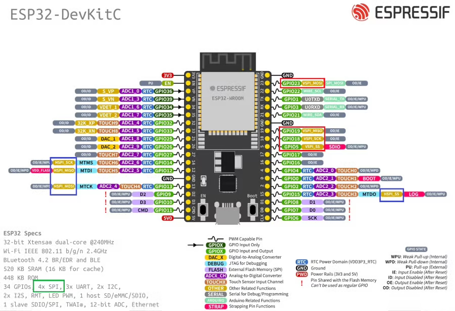
I am using the ESP32 wroom Development board with 38 pins. Below is the image showing the pinout and available SPI instances ion this board.
The ESP32 microcontroller has four Serial Peripheral Interface (SPI) ports: SPI0, SPI1, HSPI (SPI2), and VSPI (SPI3).
- SPI0 and SPI1: Used internally to communicate with the ESP32’s flash memory. These ports share the same SPI bus signals, and an arbiter determines which can access the bus.
- HSPI (SPI2) and VSPI (SPI3): General purpose SPI drivers that users can access. These ports have independent bus signals, and each bus can drive up to three SPI slaves.
The image above shows the pins availability for the VSPI (Red Box) and HSPI (Blue Box). We can use either of these instances to avoid any conflict with the internal flash memory.
SOME INFO ABOUT W25Q
I am going to use the W25Q32 for this tutorial, so I will keep the explanation limited to it. W25Q32 is a 32Megabits (4 Megabyte) SPI flash memory. It also supports the QuadSPI mode, but we are working with SPI right now. Below is the image from the datasheet explaining how the memory is arranged.
As shown above, W25Q32 has 16384 programmable pages. The number of available pages varies as per the memory. For example, W25Q16 has 8192 pages, and W25Q64 has 32768 pages. But the page size remains the same across most of the W25Q series devices. Each page occupies 256 bytes of memory and this is the maximum you can program with one program command. If you want to program more than 256 bytes, you need to send the page program command more than once.
We can erase a sector (16 Pages), 32KB Block (128 Pages), 64KB Block (128 Pages) or the entire chip at once. So a sector (16 Pages = 4KB) is the minimum size we care erase. Even if you want to update only 1 data byte, you still need to erase the entire sector. Data can not be updated without erasing the sector.
Below is the image showing the commands that we will use in this tutorial.
THE CODE
Write Enable
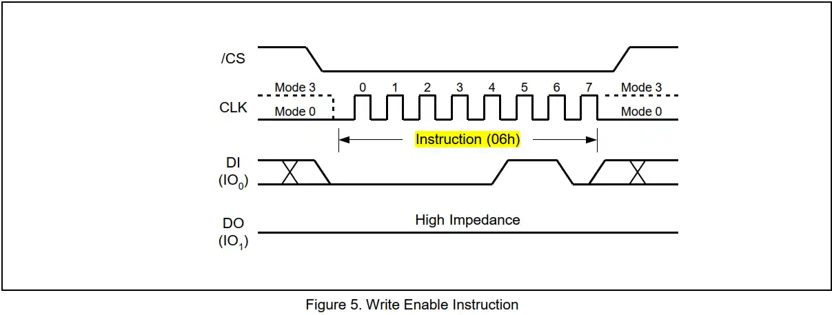
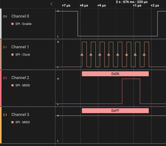
According to the datasheet, we must execute the write enable instruction before Page Program, any type of Erase and Write Status Register instruction. This is shown in the image below.
To enable the Write, we need to send the instruction 0x06 to the slave device.
Below is the function to enable the write.
void write_enable (void)
{
	uint8_t cmd = 0x06;
	SPI_Transmit(&cmd, 1);
	usleep(5000);  // wait 5ms
}We simply send the instruction (0x06) to the device. This enables the write and we can perform the page write or erasing operations after this.
The write is automatically disabled after Power-up and upon completion of the Write Status Register, Erase/Program Security Registers, Page Program, Sector Erase, Block Erase, Chip Erase and Reset instructions. Therefore we do not need to disable it manually.
Erase Sectors
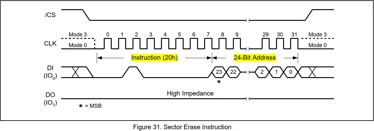
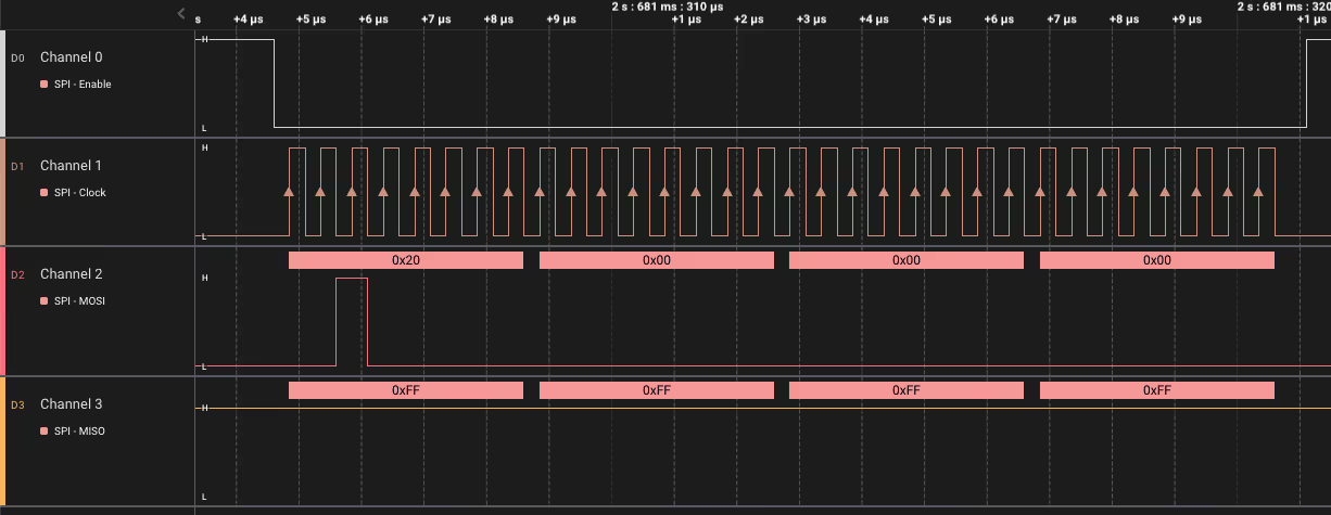
The erase sector instruction (0x20) is sent along with the memory address, whose sector should be erased. The Sector Erase instruction sets all memory within a specified sector (4K-bytes) to the erased state of all 1s (0xFF). A Write Enable instruction must be executed before the Sector Erase Instruction, otherwise device will not accept the instruction.
Below is the function to erase a specific sector.
void sector_erase (int numsector)
{
	uint8_t cmd = 0x20;
	uint32_t memAddress = numsector*16*256;  // sector num x 16 pages x 256 bytes
	uint8_t tData[10];
	tData[0] = cmd;
	tData[1] = (memAddress>>16)&0xFF;
	tData[2] = (memAddress>>8)&0xFF;
	tData[3] = (memAddress)&0xFF;

	write_enable();
	SPI_Transmit(tData, 4);
	sleep(1);
}The parameter of the function is the number of the sector, that we want to erase. The number starts from 0.
- The cmd variable stores the sector erase command, i.e. 0x20.
- Then we calculate the memory address using the sector number. Each sector contains 16 pages and each page contains 256 bytes.
- The memory address is 24bit wide for the W25Q32. Therefore we will store the address in 3 separate bytes, MSB should be stored first.
- Before sending the erase command, we need enable the write.
- To erase the sector we send the instruction followed by the memory address.
- Erasing sector takes some time, therefore we will wait for around 1 second.
Page Program
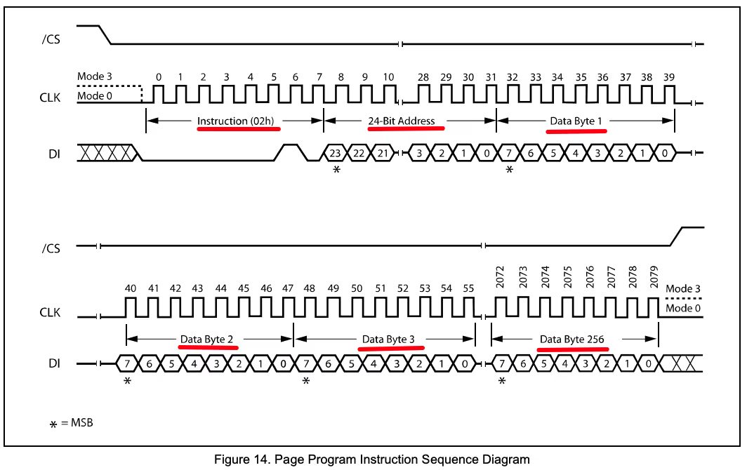
The Page Program instruction (0x02) is sent along with the memory address where the data needs to be written, followed by the data bytes. A Write Enable instruction must be executed before the Page Program Instruction, otherwise device will not accept the instruction.
Below is the function to program a page.
void write_data (int pagenum, uint8_t *datatoWrite, size_t bytes)
{
	uint8_t cmd = 0x02;
	uint32_t memAddress = pagenum*256;
	uint8_t tData[bytes+4];  // 4 additional bytes-> 1cmd, 3addr
	tData[0] = cmd;
	tData[1] = (memAddress>>16)&0xFF;
	tData[2] = (memAddress>>8)&0xFF;
	tData[3] = (memAddress)&0xFF;

	for (int i=0; i<bytes; i++)
	{
		tData[i+4] = datatoWrite[i];
	}

	write_enable();
	SPI_Transmit(tData, bytes+4);
	usleep(200000);
}The parameter of the function are as follows:
- @pagenum is the page that we want to program.
- @datatoWrite is the pointer to the data array, that we ant to write to the page.
- @bytes is the number of data bytes we want to write.
Inside this function, we will load the command, address and the data in a separate array. Then we will send the array via the SPI.
- The cmd variable stores the Page Program command, i.e. 0x02.
- Then we calculate the memory address using the sector number. Each sector contains 16 pages and each page contains 256 bytes. The memory address is 24bit wide for the W25Q32. Therefore we will store the address in 3 separate bytes, MSB should be stored first.
- Then we will store the data in the array. Since the elements 0 to 3 are already occupied by command and address, the actual data will start storing from 4th element.
- Before programming the page, we need enable the write.
- Then send the entire array using the function SPI_Transmit. The total number of bytes contains the data length (bytes) + 4 additional bytes (1 cmd + 3 Address).
- Programming page takes some time, therefore we will wait for around 200 millisecond.
Read Data
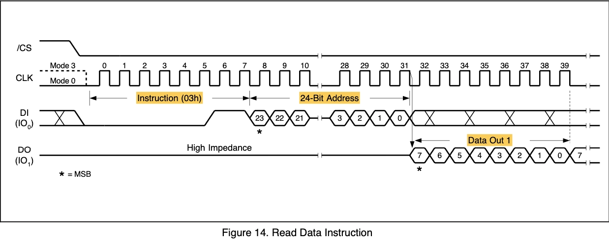
Below is the image showing the Read Instruction Sequence.
The Read Data instruction allows one or more data bytes to be sequentially read from the memory. The instruction is initiated by driving the CS pin low and then shifting the instruction code “03h” followed by a 24-bit address (A23-A0) / 32-bit address (A32-A0) into the DI pin. After the address is received, the data byte of the addressed memory location will be shifted out on the DO pin with most significant bit (MSB) first. The address is automatically incremented to the next higher address after each byte of data is shifted out allowing for a continuous stream of data. This means that the entire memory can be accessed with a single instruction as long as the clock continues. The instruction is completed by driving CS high.
Below is the function to Read data.
void read_data (int pagenum, uint8_t *buffertoStore, size_t bytes)
{
	uint8_t cmd = 0x03;
	uint32_t memAddress = pagenum*256;
	SPI_Receive(cmd, 1, memAddress, 3,  buffertoStore, bytes);
}The parameter of the function are as follows:
- @pagenum is the page that we want to read.
- @buffertoStore is the pointer to the buffer, where we want to store the received data.
- @bytes is the number of data bytes we want to read.
Inside this function, we will first calculate the memory address using the pagenum. Then pass all the parameters to the SPI_Receive function, which will receive the data.
Below is the SPI_Receive function.
void SPI_Receive (uint16_t cmd, size_t cmdLen, uint64_t Addr, size_t addrLen, uint8_t *buffertoStore, size_t dataLen)
{
    spi_transaction_t trans;
    memset(&trans, 0, sizeof(trans));

    spi_transaction_ext_t trans_ext;
    memset(&trans_ext, 0, sizeof(trans_ext));

    trans.flags = SPI_TRANS_VARIABLE_ADDR | SPI_TRANS_VARIABLE_CMD;
    trans.cmd = cmd;
    trans.addr = Addr;
    trans.rx_buffer = buffertoStore;
    trans.length = 	(dataLen)*8;

    trans_ext.address_bits = addrLen*8;
    trans_ext.command_bits = cmdLen*8;
    trans_ext.base = trans;

    if (spi_device_transmit(spi_handle, (spi_transaction_t *)&trans_ext) != ESP_OK)
    {
		printf ("writing ERROR\n");
	}
}I have already explained SPI Receive function is the previous tutorial. Although in addition to the previous explanation, here I have also added the command parameter to the function.
We already know that the ESP32 does not read the data on the MISO line when the command and address bits are being transferred. Since the W25Q slave device do need both command and address to be transferred, we will use both. The command is stored in the cmd member of the transaction structure and the command size is stored in the command_bits member of the external transaction structure.
The rest of the working of the SPI_Receive function is same as explained in the previous tutorial.
The main function
First we will define the data to be stored in the Flash memory.
char *data = "Hello world 12345";
uint8_t RxData[100];Also the RxData array will be used to store the data received from the flash memory.
void app_main(void)
{
	SPI_Init();
	sector_erase(0);
	write_data(0, (uint8_t *)data, 17);
	read_data(0, RxData, 17);
	printf ("received = %s\n", RxData);

	while (1)
	{
		sleep(2);
	}
}Inside the main function, we will first initialise the SPI.
- Then erase the sector 0. As I mentioned earlier, each sector is made up of 16 pages, therefore page 0-15 are included in sector 0.
- Next we will write the data to the page 0. We are storing 17 bytes of data.
- Then we will read the data from page 0 and store it in the RxData buffer. Again we are reading 17 bytes from the start of page 0.
- Finally we will print the received data on the terminal. The data will be printed as string.
RESULT
Below is the image showing the output of the terminal.
As you can see in the image above, the data printed on the terminal is same as what we stored in the flash memory. This means the data was successfully stored, then it was read back and printed on the terminal.
Below the images shows all the data transmission captured by the analyzer.
Sector Erase
Write Data
Read Data
PROJECT DOWNLOAD
Info
You can help with the development by DONATING Below.
To download the project, click the DOWNLOAD button.
Recommended Tools
Essential dev tools
Categories
Browse by platform

