Published: November 10, 2024
Last Updated: March 23, 2026
Last Updated: March 23, 2026
STM32 ADC Single Channel Polling Mode
In this tutorial we will learn how to use STM32 ADC in single channel polling mode. We will configure the ADC using CubeMX and HAL to read analog signals. With polling mode, the microcontroller waits until the conversion is complete and then reads the value. This method is easy to understand and works well for basic projects where you need to measure only one input. We will also test the setup on different STM32 boards and explain the example code step by step.
This is the 1st tutorial in the STM32 ADC series. I am going to use the STM32H750 based development board for this series because it has advanced ADC features. But I will also cover the configuration changes required for some of the popular series that includes STM32F103C8 and STM32F446RE.
ADC Polling Mode in STM32
What ADC Polling Mode Means
ADC polling mode in STM32 is a straightforward method of reading analog data where the CPU actively waits for the ADC conversion to finish. The microcontroller starts an ADC conversion, repeatedly checks the conversion status flag, and once the conversion is complete, reads the digital value from the ADC data register.
This approach does not use interrupts or DMA, which makes it simple and predictable. However, because the CPU is busy waiting, it is generally unsuitable for time-critical or multitasking applications.
How ADC Polling Mode Works
In polling mode, the firmware follows a simple sequence:
- Start the ADC conversion.
- Continuously check the “end of conversion” flag in a loop.
- When the flag is set, read the ADC result.
- Continue with the rest of the program.
Since the code explicitly waits for the ADC to finish, the execution flow is easy to understand and debug, which is why polling mode is often used in learning examples and basic projects.
STM32 ADC Features Across Different Boards
While the basic ADC configuration steps remain similar across STM32 families, the underlying ADC capabilities vary between series. Parameters like resolution, sampling speed, and available channels differ, which affects performance and suitable use cases.
Below is a simple comparison of ADC features across popular STM32 boards:
| STM32 Series | ADC Resolution | Sampling Speed | Channels | Typical Use Case |
|---|---|---|---|---|
| STM32F103 | 12-bit (0–4095) | Basic | Multiple | Beginner projects, simple single or multi-channel readings |
| STM32F446 | 12-bit | Faster than F1 | Multiple | Applications needing higher sampling speed and better accuracy |
| STM32H750 | 12-bit with advanced features | Very high | Multiple with advanced modes | Signal processing, real-time control, high-performance systems |
Understanding these differences helps you choose the right STM32 series and configure the ADC effectively for your project.
STM32F103 ADC Configuration
To configure ADC on STM32F103 in single channel polling mode, we will use CubeMX and HAL library. The process includes setting up the clock, enabling the ADC, and selecting the input channel.
Clock setup for STM32F103 ADC
The image below shows the clock configuration for the STM32F103C8T6.
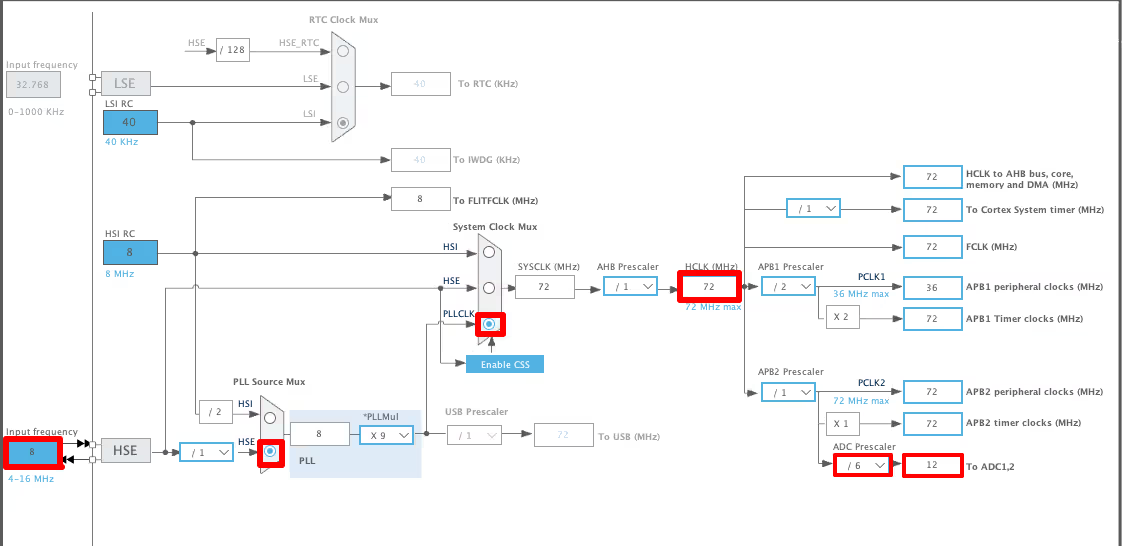
The system is clocked by the external 8MHz crystal and we can use the PLL to run the system at maximum 72 MHz. Further the ADC prescaler (6 in the image) can be used to set the ADC clock (12MHz in the image) at desired frequency.
The STM32F103C8T6 supports the ADC clock upto a maximum frequency of 14MHz.
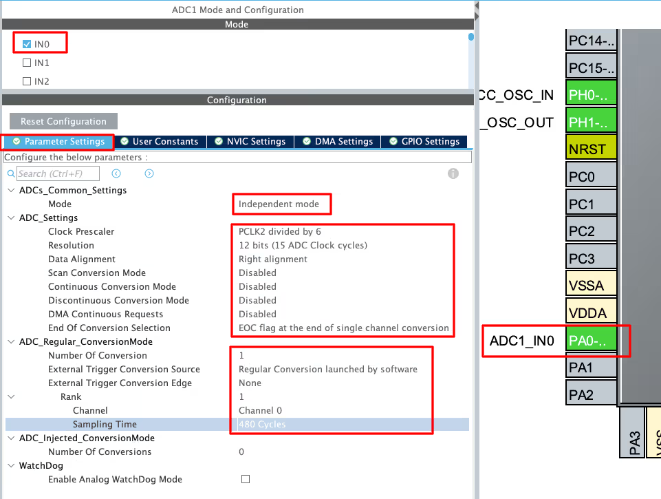
ADC Configuration
The image below shows the ADC Configuration in STM32F103C8.
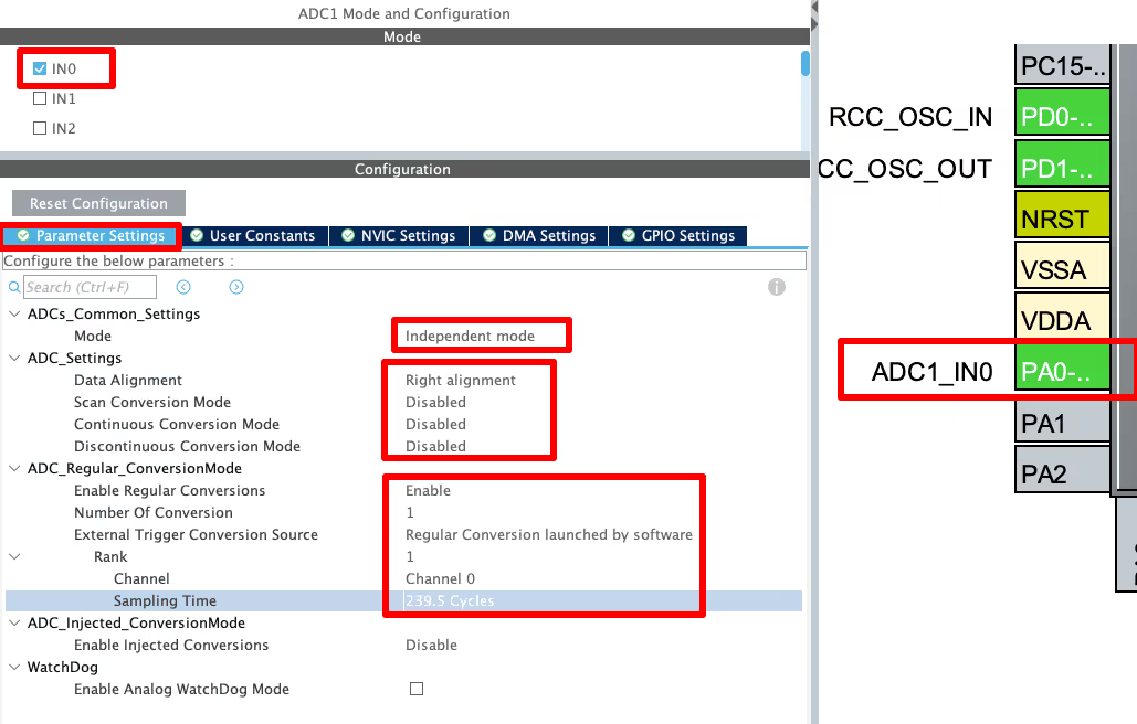
I have selected the ADC1 Channel 0 and you can see the pin PA0 is configured as the ADC1_IN0 pin. The ADC is configured in the independent mode. In this mode, the ADC1 can be used independently and we do not need any other ADC for it.
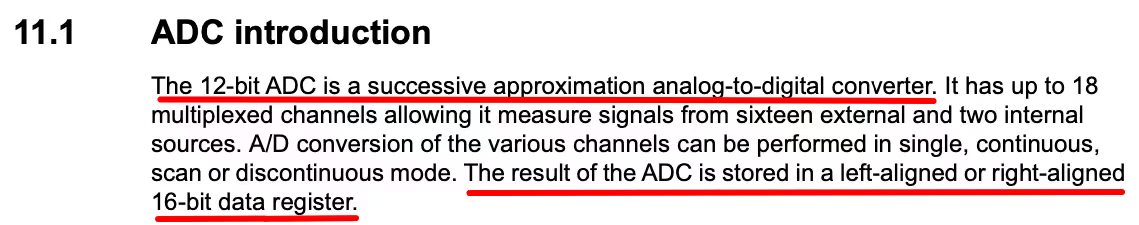
ADC Resolution
The STM32F103C8T6 ADC does not have the option to configure the ADC Resolution. By default the Resolution is 12 bit and it is fixed. You can find this information in the reference manual of the MCU. The image below is from pg 215 of the STM32F103C8 reference manual.
ADC Data Alignement
Since the ADC Resolution is 12bit, the data is stored in a 16 bit Data Register. The Data Alignment controls whether we want to align the data to the left or right of this array. The image below shows the available data alignment in STM32F103 ADC.
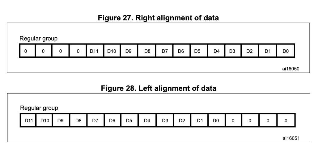
We will keep the Data alignment to the Right, as it is easier to process the data.
ADC Scan Conversion mode
This mode is used to scan a group of analog channels. This mode will be automatically selected if you are converting more than 1 channel. A single conversion is performed for each channel of the group. After each end of conversion the next channel of the group is converted automatically. If the continuousconversionmode is ENABLED, conversion does not stop at the last selected group channel but continues again from the first selected group channel.
Since we are using single channel in this tutorial, we will keep this mode disabled.
ADC Continuous conversion mode
In continuous conversion mode ADC starts another conversion as soon as it finishes one. This method is more efficient if you want to convert continuously. In case of single channel, the same channel will be converted again and again.
We are using the polling mode in this tutorial, where we will manually call the ADC to start the conversion. So we will keep this disabled for this tutorial.
ADC Regular/Injected Conversion
The ADC can be used in either the Regular conversion Mode or injected conversion mode. The Regular conversion mode is simple as it sounds, basically the normal ADC mode we use. Whereas in the injected mode, we can ‘inject’ a sequence of conversions in between the regular conversions. The injected channels has higher priority, so the ADC will pause the conversion for the regular sequence, then first convert the injected sequence, and it will resume the regular sequence afterwards.
ADC External Trigger Source
The Trigger Source can be used to start the conversion. We can use the timer’s output to trigger the ADC conversion, and hence we can also control the conversion rate. For now we will set this trigger to be launched by the software, so that we can manually start the conversion when needed.
ADC Rank
The Rank section is used to configure the individual channel. When using multiple channels, we can configure the sequence of conversion here. Also we can set the sampling time for each channel. The sampling time is set in ADC CYCLES, and the higher the cycles, the more time ADC will take to sample each channel.
I am setting the maximum sampling time as here we are using a simple potentiometer and time requirement is not an issue. To understand more about how to sample the ADC at a fixed rate, check out the ADC sampling time tutorial.
STM32F446 ADC Configuration
Clock setup for STM32F446 ADC
The image below shows the clock configuration for the ADC in STM32F446RE.
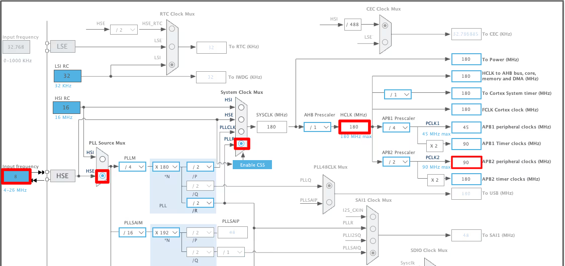
The system is clocked by the external 8MHz crystal and we can use the PLL to run the system at maximum 180 MHz. There is no separate ADC Clock shown in the clock configuration.
If we check the block diagram at pg 16 of the STM32F446RE Datasheet, we can see that the ADC1 is connected to the APB2 Clock. The image is shown below.
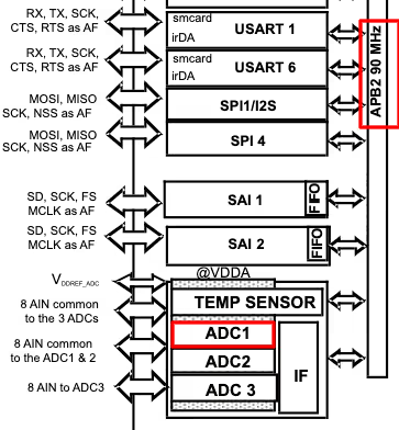
As per our current clock configuration, the APB2 clock is at 90MHz.
ADC Configuration
The image below shows the ADC configuration.
I have selected the ADC1 Channel 0 and you can see the pin PA0 is configured as the ADC1_IN0 pin. The ADC is configured in the independent mode. In this mode, the ADC1 can be used independently and we do not need any other ADC for it.
ADC Prescaler
We have the option to configure the clock Prescaler for the ADC. Our current APB2 clock is at 90MHz, and if we set the prescaler to 6, the ADC clock will be reduced to 90/6 = 15MHz.
ADC Resolution
The F446RE has the option to configure the ADC Resolution. We can set the Resolution to 6its, 8bits, 10bits or 12bits. The higher the resolution is, the more accurate will be the ADC data, but the ADC will take more time to sample and convert the result.
Here I have configured the resolution to 12bits.
The rest of the configuration is similar to what we have seen in the F103C8. We have the Data alignment, Scan conversion mode, continuous conversion mode, regular conversion, rank, sampling time etc. So I will cover the ones which are different here.
ADC DMA Continuous Request
This feature is used along with the DMA. Basically while using the DMA to fetch the data from the ADC, we can enable this feature to allow the DMA to continuously request the data from the ADC. This way we do not need to call the DMA again after it has finished receiving the data.
End of Conversion Section
The end of conversion flag (EOC) shows that the conversion is finished and the data is ready to be processed. We can choose whether this flag sets after each channel is converted or only after a sequence of channels is converted in the case of multiple channels.
Since we are using a single channel in this tutorial, either of the options are fine. But you need to be careful while using the multiple channels. This flag should be configured as according to how you want to the process the data. For example, if you are converting 10 channels and set the EOC for each channel, the interrupt will trigger 10 times for each sequence.
STM32H750 ADC Configuration
Clock setup for STM32H750 ADC
The image below shows the clock configuration for ADC in STM32H750.
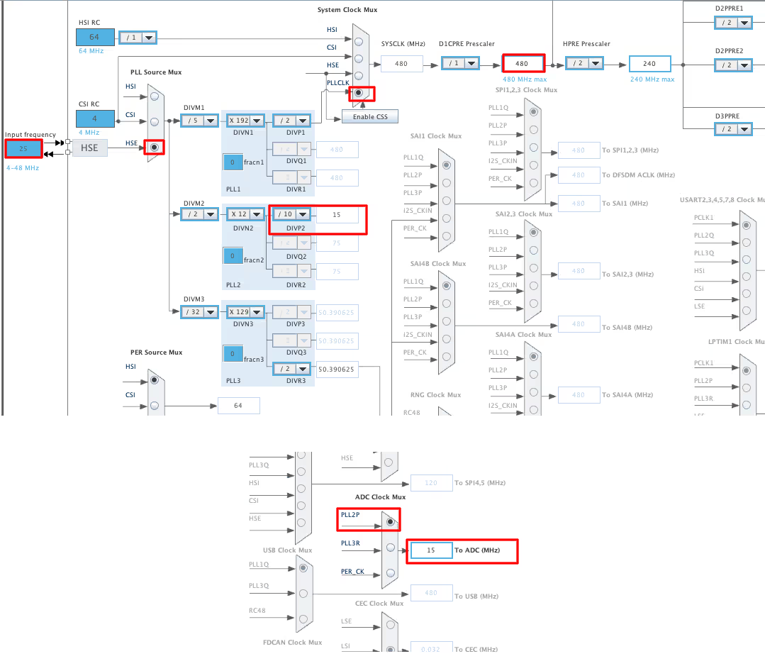
The external 25 MHz crystal clocks the system, and we use the PLL to run it at a maximum of 480 MHz. The PLL2p clocks the ADC, and we can configure it separately. With the current setup, the ADC clock runs at 15 MHz.
ADC Configuration
Below is the image showing the ADC configuration.
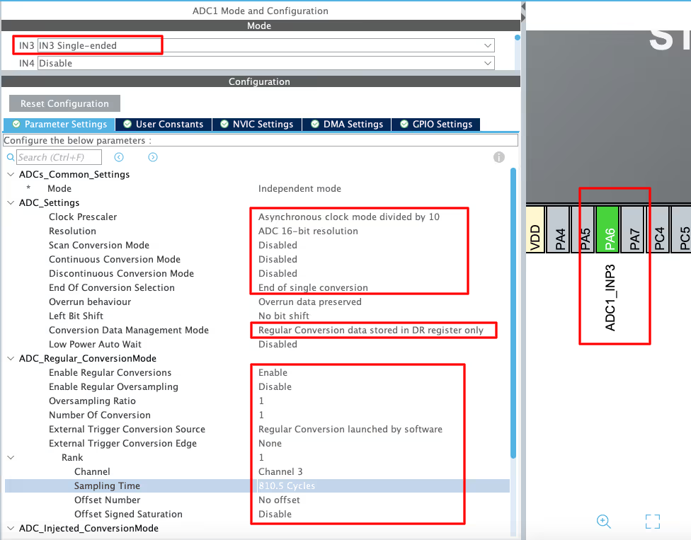
I have selected ADC1 Channel 3 in the Single Ended Mode. The single Ended mode is the Normal ADC mode we have available in the above mentioned MCUs also. In this mode, the ADC measures the voltage on the input pin. Other than this, we have another option to configure the ADC in the Differential mode. Where the ADC will measure the voltage different between the two inputs.
We will cover the differential mode in the future tutorials.
ADC Prescaler
We have the option to configure the clock Prescaler for the ADC. Our ADC clock runs at 15 MHz, and when we set the prescaler to 10, the ADC clock decreases to 1.5 MHz.
ADC Resolution
The H750 has the option to configure the ADC Resolution as well. We can set the Resolution to 8bits, 10bits, 12bits, 14bits or 16bits. The higher the resolution is, the more accurate will be the ADC data, but the ADC will take more time to sample and convert the result.
Here I have configured the resolution to 16bits.
The rest of the configuration is similar to what we have seen in the F446RE. We have the Scan conversion mode, continuous conversion mode, End of Conversion, regular conversion, rank, sampling time etc. So I will cover the ones which are different here.
Left Bit Shift
The Left Bit Shift (LSHIFT) is a way to shift the converted value towards the left. The result may be negative, so the output data is signed. We will keep it disabled for now and might cover it in the future tutorials.
Converted Data Management Mode
The mode specifies what to do with the converted data. We can transfer the converted data using the DMA, or transfer the data to the DFSDM Register (Digital Filter for Sigma-Delta Modulator) or leave the data in the ADC DR (Data Register).
We are not using the DMA transfer right now, so we will leave the data in the DR (Data Register).
ADC Oversampling
We will not cover the oversampling for now, so ignore any configuration related to that. The ADC oversampling technique is covered in a separate post.
STM32 ADC Wiring Diagram
The image below shows the connection between STM32H750 and the Potentiometer.
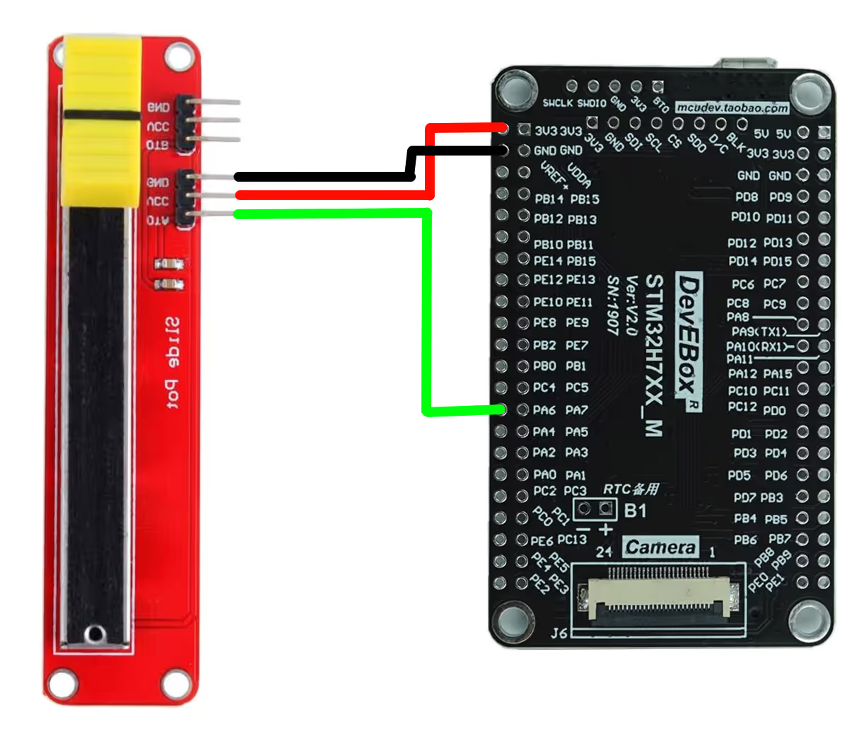
The pin connection is described in the table below.
| Potentiometer Pin | Connected To |
|---|---|
| VCC | 3.3V on STM32 |
| GND | GND on STM32 |
| OUT | PA6 (ADC1_INP3) Pin |
Example Code: Polling Mode ADC Read
This STM32 ADC example demonstrates how to read analog input using polling mode. The same code is compatible with all the STM32 MCUs. The code will remain the same for all the STM32 MCUs. If there are any changes, I will specify in this section itself.
Definitions
Let’s define some variables, which we will use in the main function later.
uint16_t ADC_VAL = 0;
int value = 0;

long map(long x, long in_min, long in_max, long out_min, long out_max)
{
  return (x - in_min) * (out_max - out_min + 1) / (in_max - in_min + 1) + out_min;
}We define ADC_VAL as a 16-bit variable, and we use it to store the converted ADC value. Even if we select 10-bit, 12-bit, or 14-bit resolution, we still declare ADC_VAL as a 16-bit variable.
We will use the map function to map the converted ADC value to our desired range. The mapped value will be stored in the value variable, which I have defined as an integer here.
The main function
Below is the main function.
int main()
{
   .....
   .....
   while (1)
   {
      HAL_ADC_Start(&hadc1);
      HAL_ADC_PollForConversion(&hadc1, 100);
      ADC_VAL = HAL_ADC_GetValue(&hadc1);
      HAL_ADC_Stop(&hadc1);
      value = map(ADC_VAL, 0, 65535, 0, 100);
      HAL_Delay (500);
   }
}We want to measure the ADC continuously, so we will write our code in the while loop. Below are the steps to get the ADC data in polling method.
- First, START the ADC.
- Next, Poll for the conversion to complete. Here I have set the timeout to 100ms. If the ADC does not finish the conversion within this time, the function will timeout.
- Then, Read the converted value and store it in the ADC_VAL variable.
- Finally, STOP the ADC.
We now have the converted data stored in the ADC_VAL variable. We will use the map function to map the converted value to 0 to 100 range. Since I have set the ADC resolution to 16bits, the maximum value of the ADC_VAL variable will be 216-1 = 65535. Similarly, the maximum value for the 12bits resolution will be 212-1 = 4095 and the same for the 10bits resolution will be 210-1 = 1023.
The while loop will run every 500ms, therefore we will keep getting the updated data continuously.
Result of STM32 ADC Single Channel Polling Mode
The gif below shows the ADC values obtained by moving the potentiometer, in the STM32CubeIDE debugger.

When you move the slider to the right, the ADC_VAL increases towards 65535 and the value variable rises towards 100. Similarly, when you move the slider to the left, the ADC_VAL decreases and the value variable drops towards 0.
Video Tutorial
STM32 ADC Polling Mode Video Tutorial
This tutorial shows how to configure and read STM32 ADC in single channel Polling mode using CubeMX. You’ll learn how to set up the ADC clock, write the code, and check results step by step. To make things even clearer, I’ve also created a video walkthrough that demonstrates the full process in action. Follow the written guide here while watching the video for a better understanding.
Watch the VideoConclusion
In this tutorial, we explored how to use the STM32 ADC in single-channel polling mode using CubeMX and the HAL library. We covered the complete configuration process, including clock setup, channel selection, and adjusting key parameters such as resolution and sampling time. The example was tested using a potentiometer, and the ADC output was verified in debugging mode to confirm correct operation.
ADC polling mode is simple to implement and ideal for understanding the fundamentals of analog-to-digital conversion in STM32. It works well for basic and low-complexity projects, but it keeps the CPU busy and is not suitable for multitasking systems. As your application grows in complexity, you can move on to more efficient approaches such as ADC using interrupts or DMA for better performance.
Browse More STM32 ADC Tutorials
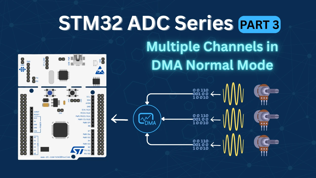
STM32 ADC Part 3 – Multiple Channels with DMA Normal Mode
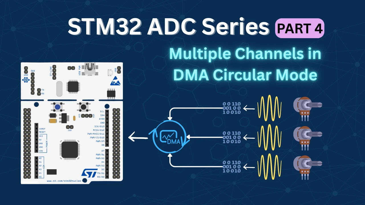
STM32 ADC Part 4 – Multiple Channels with DMA Circular Mode
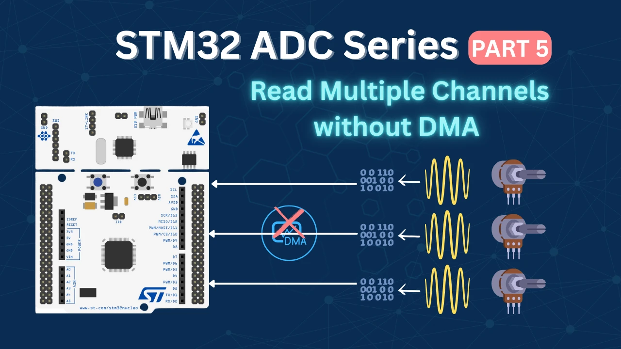
STM32 ADC Part 5 – Read Multiple‑Channel without DMA
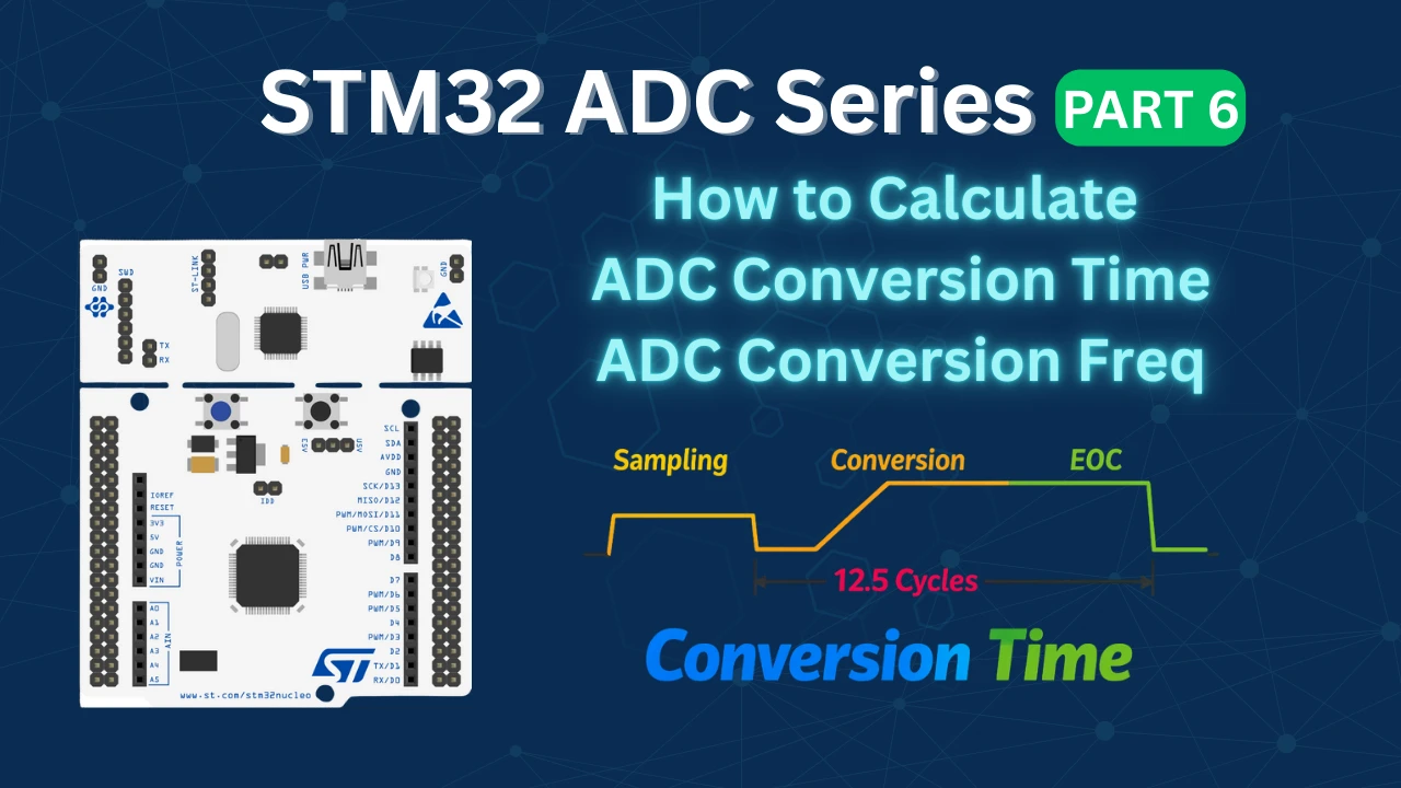
STM32 ADC Part 6 – ADC Conversion Time Explained
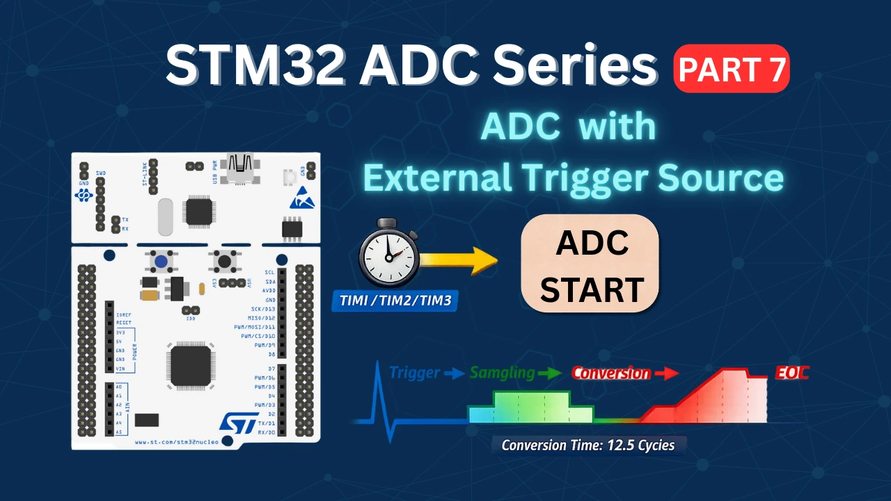
STM32 ADC PART 7 – ADC External Trigger Source Selection
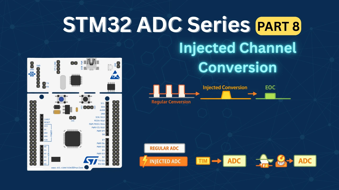
STM32 ADC Part 8 – Injected Conversion Mode
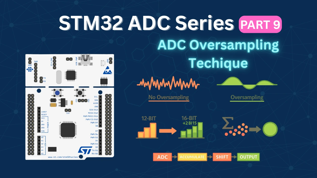
STM32 ADC Part 9 – ADC Hardware Oversampling Technique
STM32 ADC Project Download
STM32 ADC Polling Mode FAQs
Subscribe
Login
0 Comments
Newest
