Published: December 21, 2024
Last Updated: March 23, 2026
Last Updated: March 23, 2026
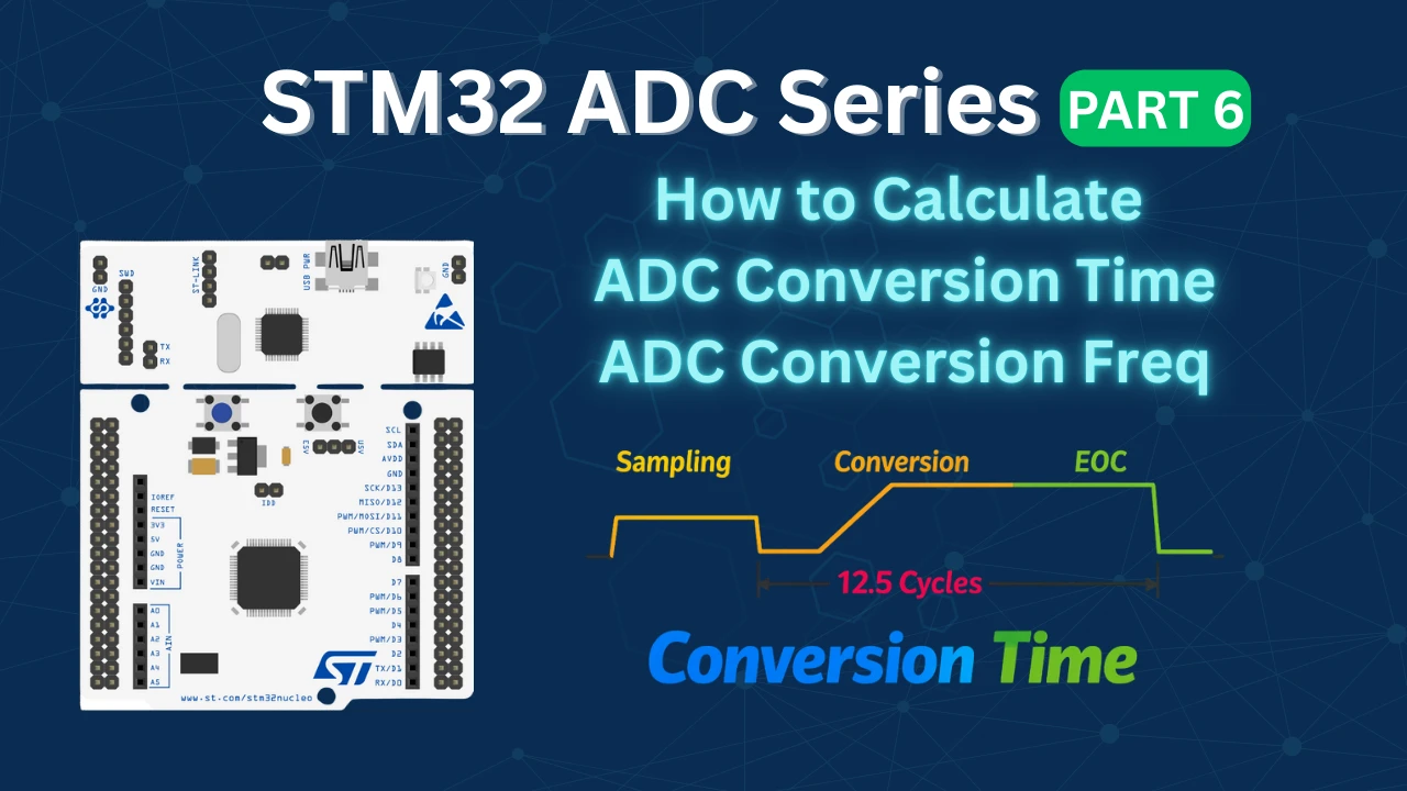
STM32 ADC Conversion Time Explained
When working with STM32 ADC, one of the most common questions is: how fast is the ADC actually converting?
In this tutorial, we’ll understand what ADC conversion time really means, what factors affect it, and how to calculate it correctly for different STM32 series. We’ll also verify the calculated values by measuring the conversion time on real hardware.
Recommended Resources:
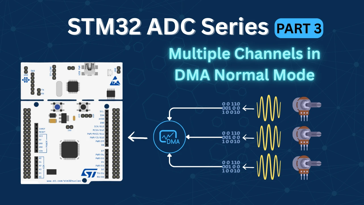
This is the 6th tutorial in the STM32 ADC series. In the previous tutorials we covered how to configure the ADC in STM32 F1, F4 and F7 series and how to use it in the single channel polling, interrupt and DMA modes to read the potentiometer data. We have also covered the Multiple channels in DMA Normal Mode, Circular Mode and Multiple Channels with DMA.
You Do not need to go through the previous tutorials in order to understand this one. But a basic knowledge of ADC configuration is needed.
Why Do We Need to Calculate ADC Conversion Time?
When using the ADC in STM32 microcontrollers, it is easy to configure the peripheral in CubeMX and start getting values without thinking much about timing. However, every ADC conversion takes a finite amount of time, and ignoring this can lead to incorrect assumptions about sampling speed, system performance, and real-time behavior. Calculating the ADC conversion time helps us understand the true limits of the ADC and design our firmware accordingly.
To Determine the Maximum Sampling Speed and System Limits
ADC conversion time directly defines how fast the ADC can sample an analog signal. Each conversion consists of a sampling phase followed by the actual conversion phase, and the total time determines the maximum achievable sampling rate.
If the ADC conversion time is longer than expected:
- Fast-changing signals may be sampled incorrectly
- High-frequency components may be lost
- The effective sampling rate may be much lower than what the application requires
This is especially important in applications such as motor control, audio processing, power monitoring, and sensor data acquisition, where timing accuracy matters. By calculating the conversion time, we can verify whether the selected ADC clock, resolution, and sampling time are suitable for the signal being measured.
It also helps in understanding trade-offs. For example, increasing resolution or sampling time improves accuracy and noise performance, but it also increases the conversion time and reduces the maximum sampling speed.
To Design Efficient and Reliable Firmware
In real applications, the ADC is often used together with timers, interrupts, and DMA. The conversion time plays a crucial role in how these components interact.
If the ADC conversion takes longer than the trigger interval:
- Timer-triggered conversions may overlap or be skipped
- Multi-channel scanning may not complete in time
- DMA buffers may not fill as expected
In polling-based ADC usage, a long conversion time can block the CPU and delay other tasks. Even in interrupt-based designs, incorrect assumptions about conversion time can cause jitter, timing violations, or unexpected system behavior.
Calculating the ADC conversion time also simplifies debugging. When ADC readings appear slow, irregular, or inconsistent, the root cause is often an incorrect clock prescaler, excessive sampling time, or an internal clock division specific to certain STM32 series. Knowing the expected conversion time makes these issues much easier to identify and fix.
Understanding the ADC Conversion Time Formula
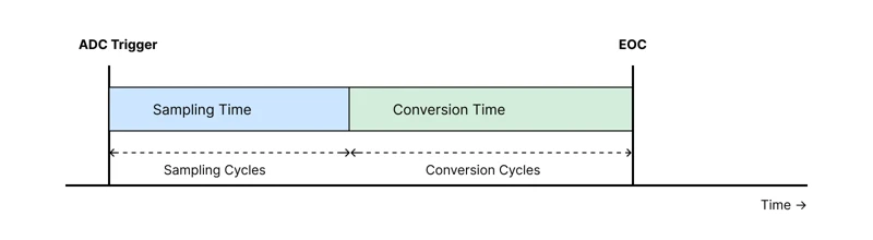
According to ST’s reference manuals, the total time required for a single ADC conversion can be calculated using the following mathematical relationship:
This formula represents the complete duration from the moment the ADC starts sampling the input signal until the digital conversion result becomes available.
Understanding the Parameters
The formula consists of three key parameters, each of which plays a critical role in determining the overall conversion time.
Sampling Cycles
Sampling cycles represent the amount of time, expressed in ADC clock cycles, during which the ADC samples the analog input signal. This value is configurable in CubeMX and can be set independently for each ADC channel.
A longer sampling time allows the internal sampling capacitor to charge more accurately, which is especially important when:
- The input source has high impedance
- Higher accuracy and stability are required
However, increasing the sampling cycles also increases the total conversion time, reducing the maximum achievable sampling rate.
Conversion Cycles
Conversion cycles represent the time, in ADC clock cycles, required by the ADC to convert the sampled analog value into a digital number. This parameter is not configurable by the user.
The number of conversion cycles depends primarily on:
- The ADC resolution selected in CubeMX
- The specific STM32 MCU family being used
Higher resolution ADC modes require more conversion cycles, resulting in longer conversion times. Since this value varies between different STM32 series, it must always be taken from the reference manual of the target microcontroller.
ADC Clock
The ADC clock is the clock signal that drives the ADC peripheral. It is derived from the system clock through one or more prescalers and directly affects the conversion speed.
A higher ADC clock reduces the total conversion time, but it is limited by the maximum ADC clock frequency specified in the datasheet. Exceeding this limit can lead to inaccurate conversions or undefined behavior.
Therefore, the ADC clock must be chosen carefully to balance speed, accuracy, and hardware constraints.
ADC Conversion Time Calculation in STM32F103C8
The STM32F103C8 microcontroller features a 12-bit ADC, and unlike some newer STM32 series, the ADC resolution is fixed and not configurable. According to the STM32F103 reference manual, a 12-bit ADC conversion requires 12.5 ADC clock cycles for the conversion phase.
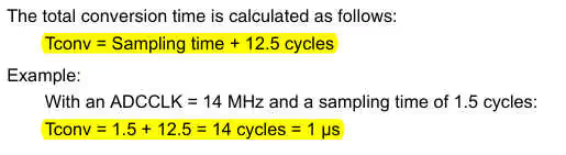
This value represents only the conversion stage and does not include the sampling time.
As discussed earlier, the total ADC conversion time is determined by three parameters:
- Sampling Cycles – configurable in CubeMX
- Conversion Cycles – fixed for a given resolution and MCU
- ADC Clock Frequency – configurable via ADC prescaler
For STM32F103C8, the conversion cycles are fixed at 12.5 cycles, while the sampling cycles and ADC clock can be configured in CubeMX.
Assumed Configuration
For this example, let us assume the following ADC configuration:
- ADC Clock = 1 MHz
- Sampling Time = 239.5 ADC cycles
- Conversion Cycles = 12.5 ADC cycles (fixed)
Step-by-Step Calculation
First, calculate the total number of ADC cycles required for one complete conversion:
Now, using the ADC clock frequency, calculate the total conversion time:
Final Result
With an ADC clock of 1 MHz and a sampling time of 239.5 cycles, the STM32F103C8 ADC requires 252 µs to complete a single conversion.
This means the maximum achievable sampling rate in this configuration is approximately:
This example clearly shows how increasing the sampling time significantly affects the total conversion time, even though the conversion cycles remain fixed.
ADC Conversion Time Calculation in STM32F446
The STM32F446RE has configurable ADC resolution. The Conversion time with respect to the resolution is mentioned in the reference manual. Below is the image from pg-368 of the reference manual of F446RE.
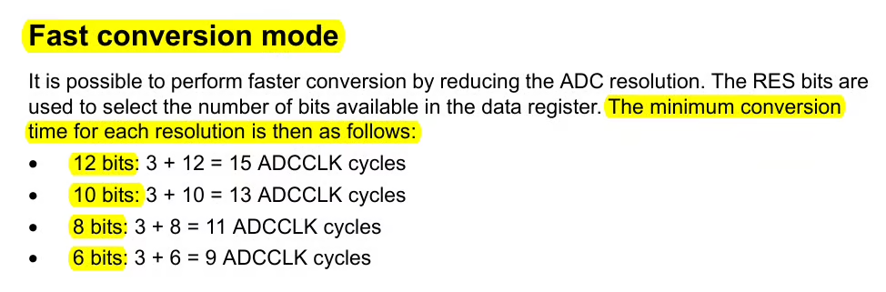
Here, the Conversion Cycles depends on the resolution you select for the ADC
- For 12 bit Resolution, Conversion CYCLES = 12
- For 10 bit Resolution, Conversion CYCLES = 10
- For 8 bit Resolution, Conversion CYCLES = 8
- For 6 bit Resolution, Conversion CYCLES = 6
Let’s understand how to configure the Resolution in STM32CubeMX.
CubeMX Configuration
We will start with the clock configuration first. The image below shows the clock configuration for F446RE.
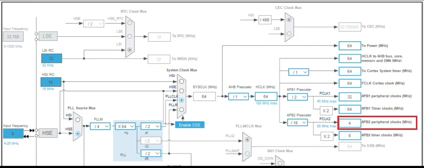
The APB2 peripheral clock is running at 4MHz. The ADC1, 2 and 3 all are connected to the APB2 Bus, therefore the ADC1 clock is also at the same frequency. We will use the prescaler to further reduce this clock.
Next we will move to the ADC configuration. The image below shows the the ADC configuration in STM32F446.
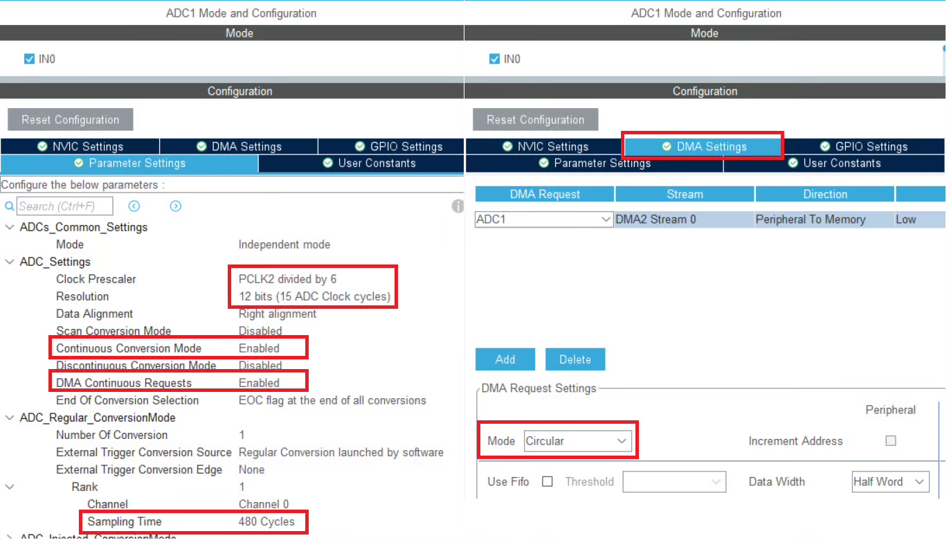
The ADC clock is derived from the APB2 clock using a prescaler. In this configuration, an ADC prescaler of 6 is selected.
Therefore, the ADC clock frequency is calculated as:
We will use the DMA to transfer the data from the ADC, therefore the DMA is enabled in circular mode. Along with DMA, the continuous conversion mode and DMA continuous request are also enabled.
The ADC Resolution is set to 12bits, therefore the conversion cycles will be 12. The ADC sampling time is configured to 480 ADC clock cycles.
Using the ADC conversion time formula, the total number of ADC cycles required for one complete conversion is calculated as:
Now, using the previously calculated ADC clock frequency:
The total ADC conversion time is:
Maximum Sampling Rate
Once the total ADC conversion time is known, the maximum achievable sampling rate can be calculated as the inverse of the conversion time.
Substituting the calculated conversion time:
We will use the pin PA1 to measure the conversion time for the ADC.

The pin PA1 is configured in the output mode. I will connect the pin PA1 to the logic analyzer, therefore the output speed of the pin is set to very high.
STM32 HAL Code to read ADC values
Inside the main function we will start the ADC in DMA mode.
uint16_t ADC_VAL;
int main()
{
  ...
  HAL_ADC_Start_DMA(&hadc1, &ADC_VAL, 1);
  while (1)
  {}
}ADC_VAL is the variable where the converted channel data will be stored and 1 is the number of channels we are converting.
Once the channel has been converted, an interrupt will trigger and the conversion complete callback will be called. Inside the callback we will toggle the pin PA1.
void HAL_ADC_ConvCpltCallback(ADC_HandleTypeDef *hadc)
{
HAL_GPIO_TogglePin(GPIOA, GPIO_PIN_1);
}The pin toggles each time the conversion is finished. Therefore the pin remains HIGH and LOW for same time, as taken by the ADC to finish the conversion. Hence the high or low time of the pin should be the same as the time we calculated using the formula.
Result showing the ADC Conversion Time
Below is the image showing the result in the logic analyzer.
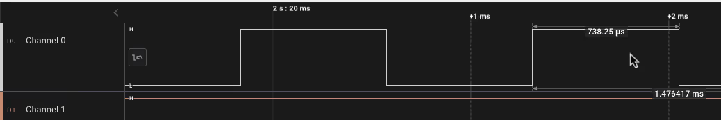
As shown above, the GPIO pin PA1 remains high for approximately 738 µs. This duration exactly matches the ADC conversion time calculated using the theoretical formula.
This confirms that the conversion time formula and the step-by-step calculation are accurate, and the measured result on real hardware aligns with the expected behavior of the ADC.
ADC Conversion Time Calculation in STM32H750
The H750 also has configurable ADC resolution. The Conversion time with respect to the resolution is mentioned in the reference manual. Below is the image from pg-952 of the reference manual of H750VB.
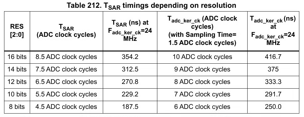
Here, the Conversion Cycles depends on the resolution you select for the ADC
- For 16 bit Resolution, Conversion CYCLES = 8.5
- For 14 bit Resolution, Conversion CYCLES = 7.5
- For 12 bit Resolution, Conversion CYCLES = 6.5
- and so on..
Let’s understand how to configure the Resolution in STM32CubeMX.
CubeMX Configuration
We will start with the clock configuration first. The image below shows the clock configuration for H750.
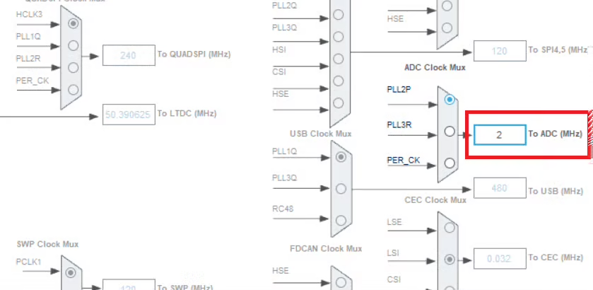
I have configured the ADC clock at 2 MHz. We will use the prescaler to reduce the clock further.
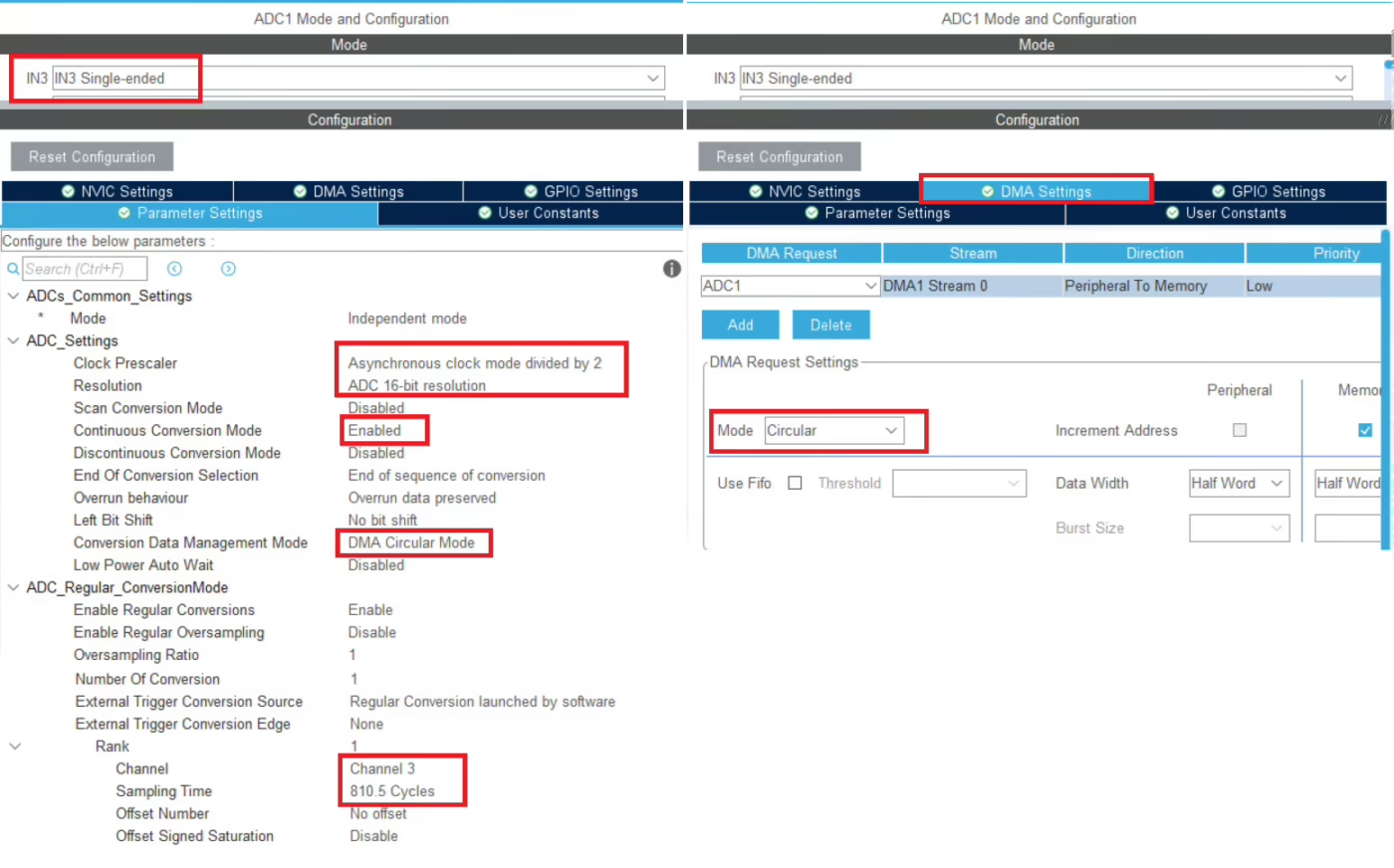
Next we will move to the ADC configuration. The image below shows the the ADC configuration in STM32H750.
The ADC clock is derived using a prescaler value of 2. Therefore, the ADC clock frequency is calculated as:
The ADC resolution is configured to 16 bits. According to the reference manual, a 16-bit conversion requires 8.5 ADC clock cycles for the conversion phase. This value is fixed and cannot be modified.
Since DMA is used to transfer the conversion data from the ADC, DMA is enabled in circular mode. In addition, continuous conversion mode is enabled, and the conversion data management is configured for circular DMA operation. This allows the ADC to continuously perform conversions without CPU intervention.
Maximum Sampling Rate
The sampling time is configured to 810.5 ADC clock cycles.
Using the ADC conversion time formula:
Substituting the values:
This calculated value represents the time required for one complete ADC conversion when operating in continuous conversion mode with circular DMA enabled.
We will use the pin PD8 to measure the conversion time for the ADC.

The pin PD8 is configured in the output mode. I will connect the pin PD8 to the logic analyzer, therefore the output speed of the pin is set to very high.
STM32 HAL Code to read ADC values
Inside the main function we will start the ADC in DMA mode.
uint16_t ADC_VAL;
int main()
{
  ...
  HAL_ADC_Start_DMA(&hadc1, &ADC_VAL, 1);
  while (1)
  {}
}
ADC_VAL is the variable where the converted channel data will be stored and 1 is the number of channels we are converting.
Once the channel has been converted, an interrupt will trigger and the conversion complete callback will be called. Inside the callback we will toggle the pin PD8.
void HAL_ADC_ConvCpltCallback(ADC_HandleTypeDef *hadc)
{
	HAL_GPIO_TogglePin(GPIOD, GPIO_PIN_8);
}The pin toggles each time the conversion is finished. Therefore the pin remains HIGH and LOW for same time, as taken by the ADC to finish the conversion. Hence the high or low time of the pin should be the same as the time we calculated using the formula.
Result showing the ADC Conversion Time
Below is the image showing the result in the logic analyzer.
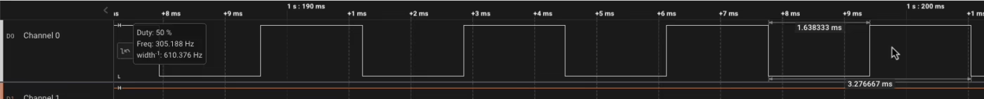
As you can see above, the pin PD8 remained high for 1.638 milliseconds. This is not what we calculated using the formula. Actually this is twice the conversion time (819uS * 2) we calculated.
The reason for it is mentioned in the reference manual of H750VB. Below is the image from pg-1036 (ADC_CCR Register).
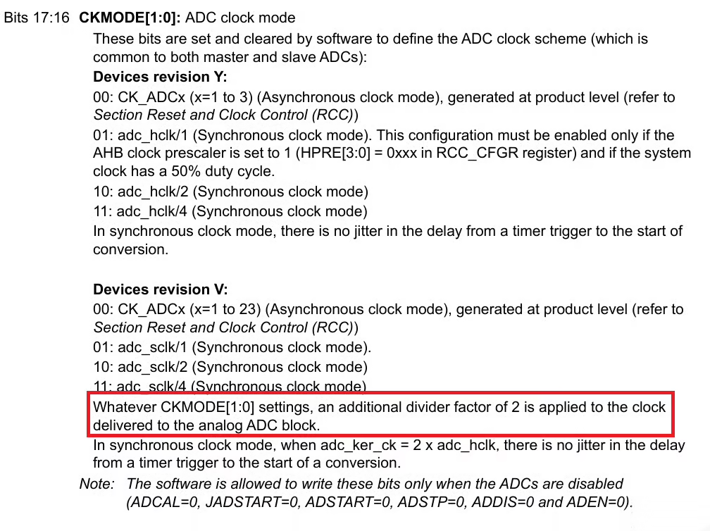
As stated in the reference manual, STM32 devices with revision V apply an additional divide-by-2 factor to the ADC clock. This means the effective ADC clock is halved, and consequently, the total ADC conversion time becomes twice the value calculated previously.
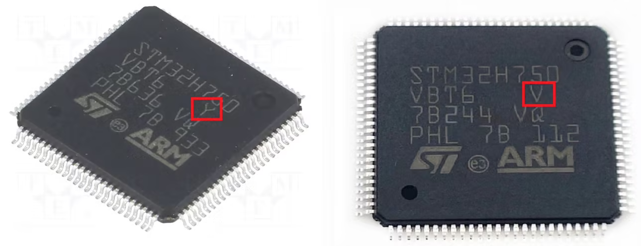
It is important to verify the device revision of the MCU you are using, because different revisions may have different internal ADC clock behavior.
For revision V devices, the formula for the total ADC conversion time should be modified to account for this divide factor:
This ensures accurate calculation of conversion time for revision V MCUs.
The table below shows the ADC clock connection with the MCU Revision.
| MCU Series | Revision | ADC Clock Behavior |
|---|---|---|
| STM32F7 | V | ADC clock divided by 2 → conversion time ×2 |
| STM32F7 | U or earlier | Normal ADC clock → use standard formula |
| STM32H7 | V | ADC clock divided by 2 → conversion time ×2 |
| STM32H7 | Other | Normal ADC clock → use standard formula |
Video Tutorial
STM32 ADC Conversion Time – Video Tutorial
In this tutorial, we explain how to calculate the ADC conversion time on STM32 microcontrollers. You’ll learn about sampling cycles, conversion cycles, ADC clock, and how they affect total conversion time. The video also demonstrates step-by-step calculations, real measurements on hardware, and tips for using DMA and continuous conversion modes.
Watch the VideoConclusion
In this tutorial, we explored ADC conversion time in STM32 microcontrollers in detail. We started by understanding why knowing the conversion time is important, including its impact on sampling speed, real-time applications, and system design. We then introduced the formula to calculate total conversion time, explained all its parameters—sampling cycles, conversion cycles, and ADC clock—and demonstrated step-by-step calculations for different STM32 MCUs. We also covered practical aspects like prescalers, DMA in circular mode, continuous conversion, and special cases for revision V devices where the ADC clock is internally divided.
Understanding ADC conversion time is crucial for designing efficient, accurate, and reliable systems. By calculating conversion time and maximum sampling rate, developers can choose the right sampling settings, avoid timing issues, and ensure that their firmware handles ADC data correctly—whether using polling, interrupts, or DMA. This knowledge not only helps optimize performance but also makes debugging and system design much more predictable, especially for real-time applications such as motor control, audio processing, or sensor monitoring.
Browse More STM32 ADC Tutorials
STM32 ADC Part 4 – Multiple Channels with DMA Circular Mode
STM32 ADC Part 5 – Read Multiple‑Channel without DMA
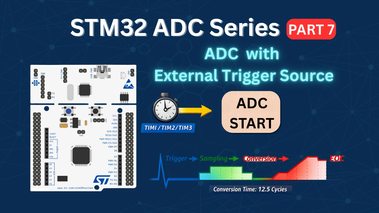
STM32 ADC PART 7 – ADC External Trigger Source Selection
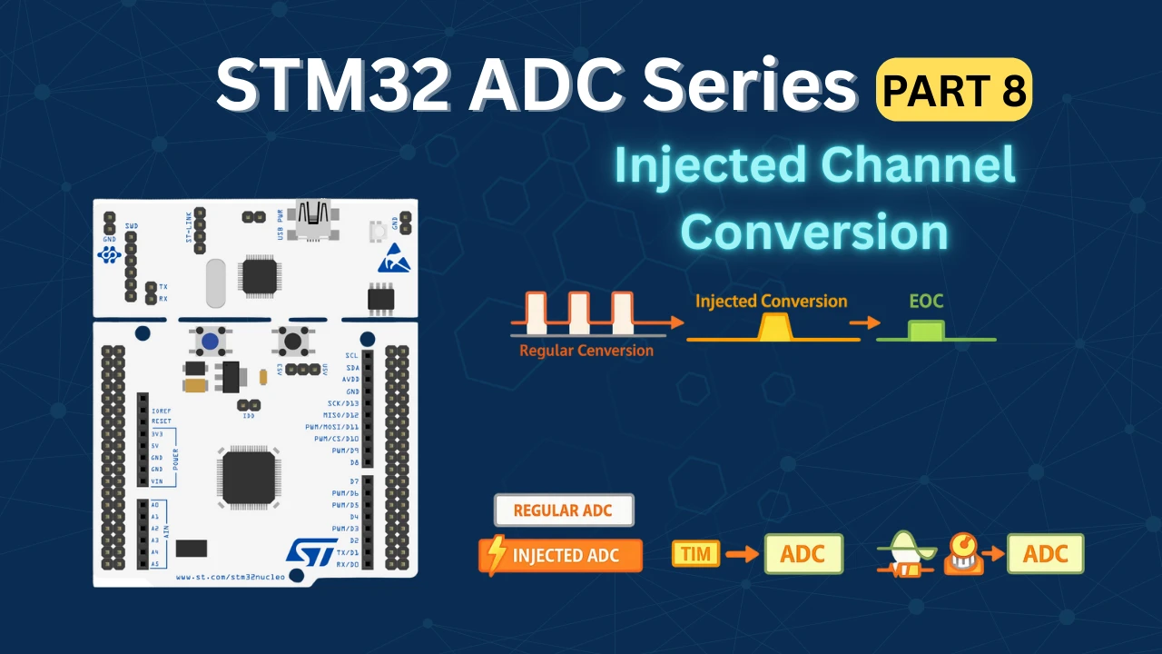
STM32 ADC Part 8 – Injected Conversion Mode
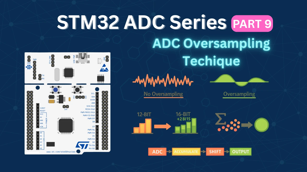
STM32 ADC Part 9 – ADC Hardware Oversampling Technique
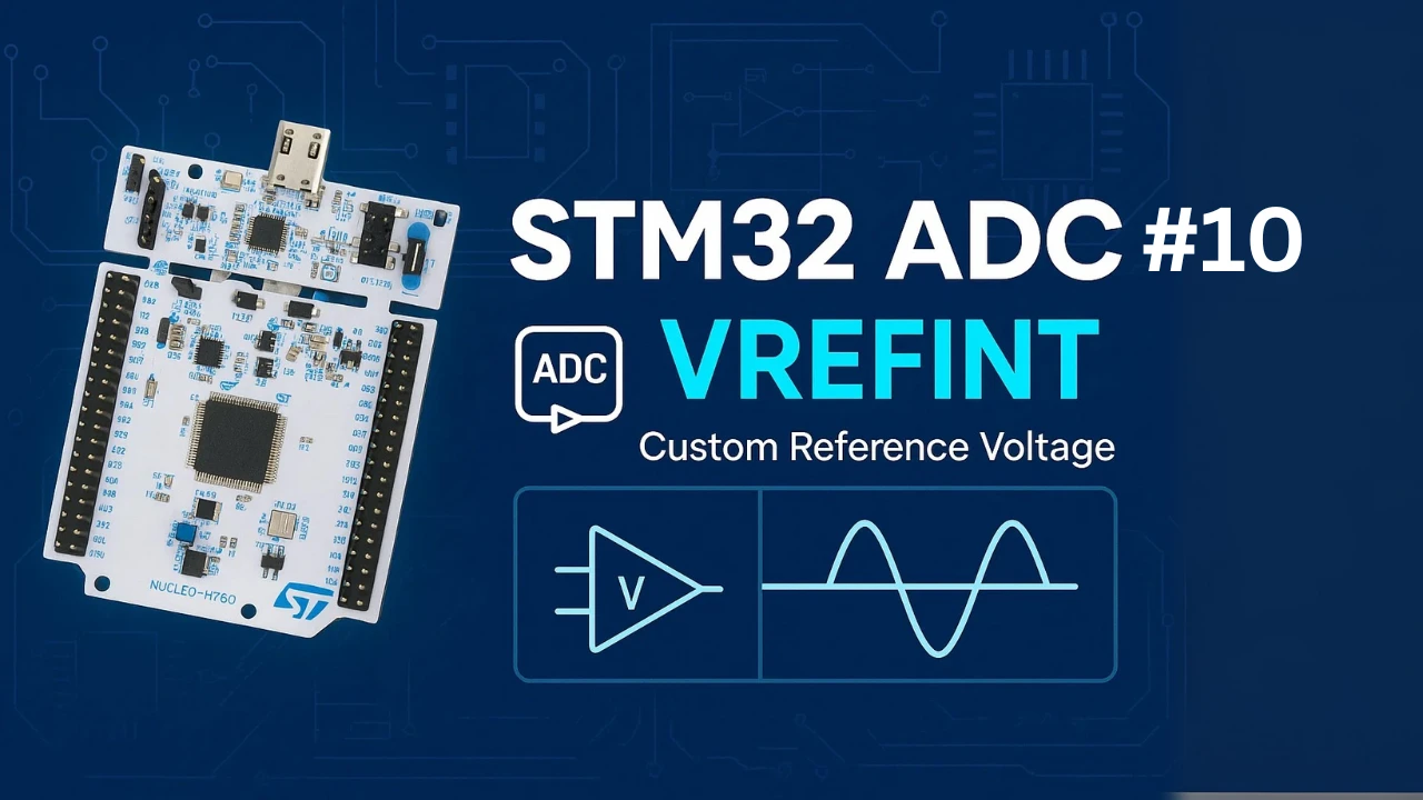
STM32 ADC Part 10 – How to use ADC Reference Voltage

No code download for this video???