Updated On: February 6, 2026
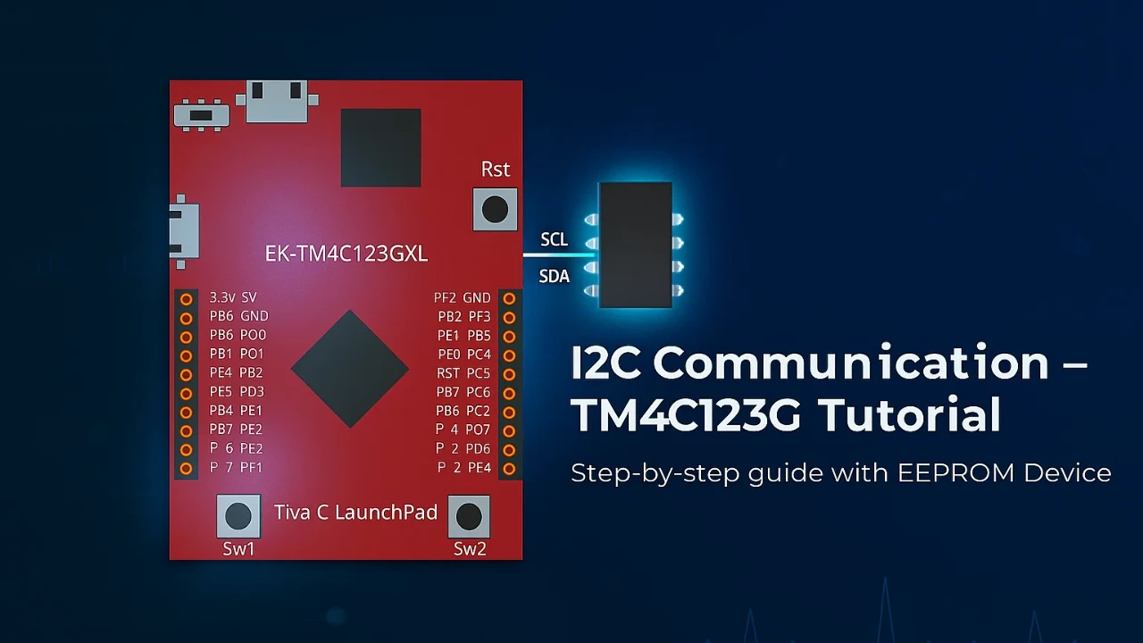
I2C Communication in TM4C123G Tiva C LaunchPad Using TivaWare
In this tutorial, we will learn how to use the I2C peripheral in TM4C123G Tiva C LaunchPad using TivaWare APIs.
I2C (Inter-Integrated Circuit) is one of the most popular serial communication protocols used in embedded systems. It allows multiple devices to communicate over just two wires – SDA and SCL.
We will start by understanding how I2C works, explore the I2C modules available in TM4C123G, and then configure the peripheral step-by-step using TivaWare. Finally, we will connect a simple EEPROM (24C02) to verify that our I2C read and write functions are working correctly.
Recommended Resources:
I have already covered how to create a project in CCStduio and configure system clock in the previous tutorials. This tutorial is going to be a continuation in this series, so you must read the following tutorials first:
- How to Setup CCStudio and build your first project with TM4C123G
- How to configure system clock in TM4C123G
Introduction to I2C Communication
What is I2C Protocol
I2C (Inter-Integrated Circuit) is a serial communication protocol that allows multiple devices to communicate using only two wires, SDA (Serial Data) and SCL (Serial Clock). It was developed by Philips (now NXP) and is widely used in microcontrollers, sensors, memory chips, and display modules.
The I2C protocol follows a master–slave architecture.
- The master controls the clock and initiates communication.
- The slave responds when addressed by the master.
Each I2C device has a unique 7-bit or 10-bit address, which allows multiple devices to share the same bus without conflict.
Data transfer happens in packets of 8 bits (1 byte), and each byte is followed by an ACK (acknowledge) or NACK (not acknowledge) signal.
Because of its simple design, I2C has become the standard communication method for many low-speed peripherals like temperature sensors, EEPROMs, RTCs, and LCD drivers.
Features of I2C Communication
Here are some key features of the I2C protocol that make it so popular in embedded systems:
- Two-wire communication using only SDA and SCL lines.
- Multiple devices can be connected on the same bus (multi-slave support).
- Supports both 7-bit and 10-bit addressing modes.
- Communication is bidirectional — the same bus can send and receive data.
- Speed modes:
- Standard mode – 100 kbps
- Fast mode – 400 kbps
- Fast mode plus – 1 Mbps
- High-speed mode – up to 3.4 Mbps
- Requires pull-up resistors on both SDA and SCL lines.
- Provides ACK/NACK mechanism for reliable communication.
The master controls all timing, so slaves don’t need to generate their own clock signals. This makes hardware implementation easier.
Why Use I2C in Embedded Systems
I2C is widely used in embedded systems because it offers a good balance between simplicity, flexibility, and low pin count.
Here are the main reasons why developers prefer I2C:
- It requires only two wires, which saves microcontroller pins.
- You can connect multiple devices (sensors, memory, displays) using the same bus.
- The protocol supports address-based communication, so each device can be uniquely identified.
- Hardware support for I2C is available in almost all microcontrollers, including the TM4C123G Tiva C LaunchPad.
- It’s perfect for medium-speed, short-distance communication, such as onboard sensor networks or peripheral expansion.
Basics of I2C Communication
Understanding how data transfers happen on the I2C bus helps you read and debug signals easily.
I2C uses only two open-drain lines:
- SCL (Serial Clock Line) – generated by the master.
- SDA (Serial Data Line) – used to send and receive data.
Both lines stay HIGH when the bus is idle. Communication begins when the master issues a START condition and ends with a STOP condition.
Start and Stop Conditions in I2C
Every I2C communication starts with a START and ends with a STOP.
- START condition (S) → SDA goes LOW while SCL is HIGH.
- STOP condition (P) → SDA goes HIGH while SCL is HIGH.
Timing Diagram: START and STOP Conditions:
SCL:  ────────┐┌──────┐┌──────┐┌──────┐┌──────
SDA:  ────────┘└───────────────┘└─────────────
↑Start condition ↑Stop conditionIn this diagram:
- The falling edge of SDA while SCL is HIGH = START.
- The rising edge of SDA while SCL is HIGH = STOP.
I2C Address Frame
After the START, the master sends an 8-bit address frame:
- 7 bits for the slave address.
- 1 bit for the R/W flag (0 = Write, 1 = Read).
Timing Diagram: Address Frame:
SCL: ─┐ ┌─ ┐ ┌─ ┐ ┌─ ┐ ┌─ ┐ ┌─ ┐ ┌─ ┐ ┌─ ┐ ┌─ ┐
SDA: ─┴─A6─A5─A4─A3─A2─A1─A0─R/W─┴────────────
↑ ACK/NACK bitAfter the 8 bits, the slave pulls SDA LOW to send an ACK. If the slave doesn’t exist or is busy, SDA stays HIGH (NACK).
Acknowledgment (ACK) and Not Acknowledgment (NACK)
The ACK signal confirms successful data transfer. After every 8-bit byte, the receiver sends 1 extra clock pulse to signal ACK/NACK.
Timing Diagram: ACK and NACK:
SCL: ─┐ ┌─ ┐ ┌─ ┐ ┌─ ┐ ┌─ ┐ ┌─ ┐ ┌─ ┐ ┌─ ┐ ┌─ ┐
SDA: ─D7 D6 D5 D4 D3 D2 D1 D0  ┴───────────────
↓ ACK = SDA LOWIf SDA remains HIGH during the 9th clock pulse → NACK.
Data Write Operation (Master → Slave)
In a write sequence:
- Master sends START.
- Sends slave address + Write bit (0).
- Slave sends ACK.
- Master sends data bytes.
- Each byte is followed by ACK from the slave.
- Master sends STOP.
Timing Diagram: Write Operation:
SCL: ─┐┌─┐┌─┐┌─┐┌─┐┌─┐┌─┐┌─┐┌─┐┌─┐┌─┐┌─┐
SDA: ─S Address+W ACK Data1 ACK Data2 ACK P─
↑Start ↑StopEach ACK ensures the slave received the byte correctly.
Data Read Operation (Master ← Slave)
During a read:
- Master sends START.
- Sends slave address + Read bit (1).
- Slave sends ACK.
- Slave transmits data bytes.
- Master sends ACK after each byte (to read more).
- After the last byte, master sends NACK and a STOP.
Timing Diagram: Read Operation:
SCL: ─┐┌─┐┌─┐┌─┐┌─┐┌─┐┌─┐┌─┐┌─┐┌─┐┌─┐┌─┐
SDA: ─S Address+R ACK Data1 ACK Data2 NACK P─
↑Start ↑StopThe final NACK tells the slave that no more data is needed.
Repeated Start Condition
A Repeated START is used when the master wants to change direction (e.g., write, then read) without releasing the bus. It looks like another START condition, but it happens before the STOP.
Timing Diagram: Repeated START:
SCL: ─────┐┌────┐┌────┐┌────┐┌────┐┌────┐┌────
SDA: ─────┘└────────┘└──────┘└───────────────
↑Start ↑Repeated Start ↑StopRepeated START keeps control of the bus and prevents other masters from interrupting.
Summary of I2C Signals
| Condition | Description | SDA & SCL Behavior |
|---|---|---|
| START | Begin communication | SDA ↓ while SCL ↑ |
| STOP | End communication | SDA ↑ while SCL ↑ |
| ACK | Byte received successfully | SDA LOW on 9th clock |
| NACK | Byte not acknowledged | SDA HIGH on 9th clock |
| Repeated START | Change direction without releasing bus | SDA ↓ while SCL ↑ again |
I2C Peripheral in TM4C123G Tiva C LaunchPad
The TM4C123G Tiva C LaunchPad comes with four I2C modules – I2C0, I2C1, I2C2, and I2C3. Each module can work as a master or a slave, depending on your application. These modules are independent of each other, which means you can use multiple I2C buses at the same time.
| I2C Module | Base Address | Function |
|---|---|---|
| I2C0 | 0x4002.0000 | Master/Slave |
| I2C1 | 0x4002.1000 | Master/Slave |
| I2C2 | 0x4002.2000 | Master/Slave |
| I2C3 | 0x4002.3000 | Master/Slave |
Each module uses a separate set of pins, so you can choose the one that fits your project layout. For simple projects or testing, I2C0 is most commonly used because its pins are easy to access on the LaunchPad headers.
I2C Pin Mapping and Alternate Functions
Each I2C module on the TM4C123G uses two pins – one for SCL (clock) and one for SDA (data). These pins are multiplexed with GPIO pins, so you must configure them to use their alternate I2C functions.
Here’s a quick reference for all I2C modules and their default pin mapping:
| I2C Module | SCL Pin | SDA Pin | GPIO Port |
|---|---|---|---|
| I2C0 | PB2 | PB3 | Port B |
| I2C1 | PA6 | PA7 | Port A |
| I2C2 | PE4 | PE5 | Port E |
| I2C3 | PD0 | PD1 | Port D |
When using TivaWare, these pins are configured using the GPIOPinConfigure() function.
For example, if you use I2C0, you’ll need to call:
GPIOPinConfigure(GPIO_PB2_I2C0SCL);
GPIOPinConfigure(GPIO_PB3_I2C0SDA);Then you set the pin type as I2C:
GPIOPinTypeI2CSCL(GPIO_PORTB_BASE, GPIO_PIN_2);
GPIOPinTypeI2C(GPIO_PORTB_BASE, GPIO_PIN_3);Don’t forget to connect 4.7 kΩ or 10 kΩ pull-up resistors to both SDA and SCL lines. I2C is an open-drain bus, so it needs external pull-ups to work correctly.
Clock Configuration and Speed Modes
The I2C peripheral in TM4C123G can operate in multiple speed modes depending on your system clock and configuration.
You can choose between:
- Standard Mode – 100 kbps
- Fast Mode – 400 kbps
- Fast Mode Plus – 1 Mbps
- High-Speed Mode – up to 3.4 Mbps (Master only)
The clock frequency for I2C is derived from the system clock. You can initialize the I2C peripheral with the I2CMasterInitExpClk() function:
I2CMasterInitExpClk(I2C0_BASE, SysCtlClockGet(), false);The last parameter sets the speed:
false→ standard mode (100 kbps)true→ fast mode (400 kbps)
So, for a basic test or communication with EEPROM, standard mode (100 kbps) is more than enough and ensures stable operation.
Hardware Setup for I2C Testing
Before testing the I2C code on the TM4C123G Tiva C LaunchPad, we need to connect it to an external I2C device. Here we’ll use the 24C256 EEPROM, a popular and easy-to-use I2C-based memory chip. It’s perfect for testing I2C write and read operations, as it always responds to valid I2C commands.
AT25C256 Pinout
Before wiring the AT25C256 EEPROM, let’s understand its pin configuration. The chip usually comes in an 8-pin package, and each pin has a specific function.
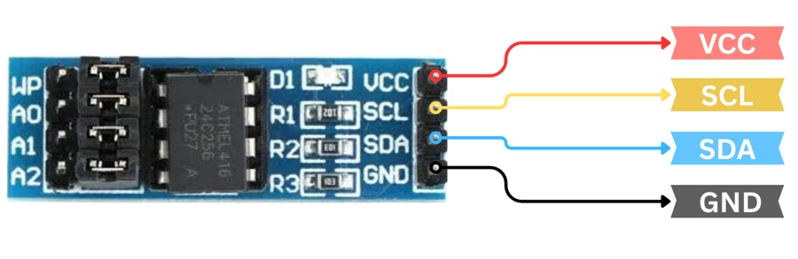
The table below shows the pin description for each pin:
| Pin | Name | Description |
|---|---|---|
| 4 | GND | Ground connection |
| 5 | SDA | Serial Data – I2C data line |
| 6 | SCL | Serial Clock – I2C clock line |
| 8 | VCC | Power supply pin (1.7V to 5.5V) |
The A0, A1, and A2 pins allow you to select the device address when using multiple EEPROMs on the same I2C bus. The WP pin can be tied to GND to allow write operations or connected to VCC to protect the EEPROM from accidental writes.
Note: In the AT24C256 module shown in the image above, the pins A0, A1, A2 and WP are connected to the ground by default.
Connecting TM4C123G to an I2C Device (EEPROM 24C256)
The 24C256 is a 256 Kbit (32 KByte) serial EEPROM that uses the I2C bus for communication. It supports both Standard (100 kHz) and Fast (400 kHz) modes.
We’ll connect it to the I2C0 module of the TM4C123G, which uses PB2 (SCL) and PB3 (SDA).
| EEPROM Pin | Description | TM4C123G Pin | Notes |
|---|---|---|---|
| VCC | Power supply | 3.3V | Can also operate at 5V |
| GND | Ground | GND | Common ground with MCU |
| SCL | Serial Clock | PB2 | I2C0SCL |
| SDA | Serial Data | PB3 | I2C0SDA |
When all three address pins (A0, A1, A2) are tied to GND, the base address of the 24C256 becomes:
Device Address = 0b1010000 = 0x50 (7 Bit)Note: The three address bits (A2–A0) allow you to connect up to 8 EEPROMs (0x50–0x57) on the same I2C bus if you ever need more memory.
Connection Summary:
The image below shows the connection between AT24C256 EEPROM Module and TM4C123G.
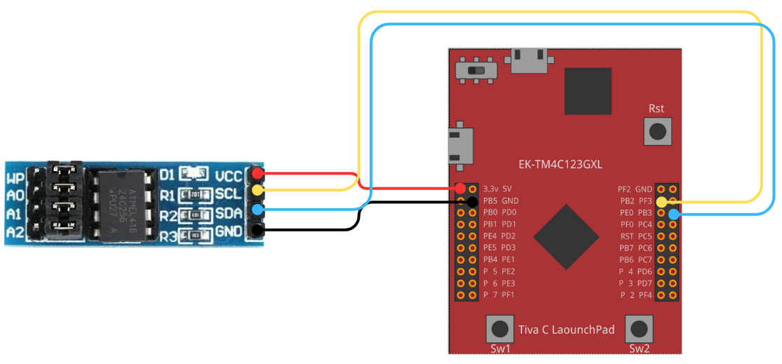
The connection is as follows:
TM4C123G (I2C0) EEPROM 24C256
-----------------------------------
3.3V ----------> VCC
PB2 (SCL) ----------> SCL
PB3 (SDA) ----------> SDA
GND ----------> GNDPull-up Resistors and Power Supply
The I2C bus requires pull-up resistors on both SDA and SCL lines. This is because the I2C interface uses open-drain drivers, which can pull the line LOW but not HIGH.
Use two resistors:
- 4.7 kΩ → suitable for 100 kHz speed.
- 2.2 kΩ → for higher-speed (400 kHz) communication.
Connect them as follows:
3.3V ---/\/\/\--- SDA (PB3)
3.3V ---/\/\/\--- SCL (PB2)
(4.7kΩ each)Make sure both the EEPROM and MCU share a common ground and are powered by the same voltage level (3.3V). This ensures proper logic level compatibility and stable communication.
Note: Some I²C breakout boards already have built-in pull-up resistors. Check the board before adding external ones, as extra resistors can cause signal issues.
Setting Up I2C Peripheral Using TivaWare
To use the I2C peripheral on the TM4C123G Tiva C LaunchPad, we will configure the hardware and enable it through TivaWare APIs. TivaWare provides easy-to-use functions to initialize and control I2C, so you don’t have to deal directly with low-level register programming.
Let’s go step-by-step through the setup process.
Header Files Used
Let’s start with the header files to be used in this project.
#include <stdint.h>
#include <stdbool.h>
#include "inc/hw_memmap.h"
#include "driverlib/sysctl.h"
#include "driverlib/i2c.h"
#include "driverlib/gpio.h"
#include "driverlib/pin_map.h"<stdint.h>– Defines fixed-width data types likeuint8_t,uint16_t,uint32_t.<stdbool.h>– Adds Boolean typesbool,true, andfalse."inc/hw_memmap.h"– Contains base addresses of all peripherals (I2C, GPIO, UART, etc.)."driverlib/sysctl.h"– Used for system setup and enabling peripheral clocks."driverlib/i2c.h"– Provides all I2C driver functions from TivaWare."driverlib/gpio.h"– Configures and controls GPIO pins."driverlib/pin_map.h"– Maps pins to their alternate hardware functions (like PB2 → I2C0SCL).
Enabling Clock for I2C and GPIO Modules
The first step in any peripheral initialization is to enable the clock for both the I2C module and its corresponding GPIO port.
The TM4C123G has four I2C modules (I2C0–I2C3). Each module is connected to specific GPIO pins. For example, I2C0 uses PB2 (SCL) and PB3 (SDA).
To enable the clock for these modules, use the following TivaWare APIs:
SysCtlPeripheralEnable(SYSCTL_PERIPH_I2C0); // Enable I2C0 module
SysCtlPeripheralEnable(SYSCTL_PERIPH_GPIOB); // Enable GPIO port BAfter enabling the clock, it’s a good practice to wait until the peripheral is ready:
while(!SysCtlPeripheralReady(SYSCTL_PERIPH_I2C0));
while(!SysCtlPeripheralReady(SYSCTL_PERIPH_GPIOB));This ensures that both modules are powered up and ready for configuration before moving ahead.
Configuring SDA and SCL Pins
Next, we configure the GPIO pins for I2C functionality. Each I2C pin supports alternate functions (since GPIO pins can serve multiple peripherals).
For I2C0, the pin mapping is:
| Signal | Pin | Function |
|---|---|---|
| I2C0SCL | PB2 | Clock line |
| I2C0SDA | PB3 | Data line |
Here’s how to configure them:
GPIOPinConfigure(GPIO_PB2_I2C0SCL);
GPIOPinConfigure(GPIO_PB3_I2C0SDA);
GPIOPinTypeI2CSCL(GPIO_PORTB_BASE, GPIO_PIN_2);
GPIOPinTypeI2C(GPIO_PORTB_BASE, GPIO_PIN_3);Note:
- The
GPIOPinConfigure()function maps the pin to its I2C alternate function. GPIOPinTypeI2CSCL()andGPIOPinTypeI2C()set the electrical characteristics needed for I2C operation.
Initializing I2C Master and Slave Modes
Once the pins are configured, the I2C module itself must be initialized in either Master or Slave mode. In most applications, the microcontroller (TM4C123G) acts as the Master, while the peripheral device (like an EEPROM or sensor) acts as the Slave.
To initialize the I2C Master:
I2CMasterInitExpClk(I2C0_BASE, SysCtlClockGet(), false);Here:
I2C0_BASE→ selects I2C0 module.SysCtlClockGet()→ provides the system clock frequency.false→ sets the communication speed to 100 kbps (Standard Mode).
Set it totruefor 400 kbps (Fast Mode).
To initialize as a Slave (if needed):
I2CSlaveInit(I2C0_BASE, 0x3C); // Slave address 0x3CThis configures the device to respond to master requests sent to address 0x3C.
Complete I2C Initialization Code
Below is the complete function to initialize the I2C0 module and configure the GPIO pins PB2 (SCL) and PB3 (SDA) for I2C communication.
#include <stdint.h>
#include <stdbool.h>
#include "inc/hw_memmap.h"
#include "driverlib/sysctl.h"
#include "driverlib/i2c.h"
#include "driverlib/gpio.h"
#include "driverlib/pin_map.h"
//*********************************************************
// Function: I2C0_Init
// Description: Initializes I2C0 module on TM4C123G for Master mode
//*********************************************************
void I2C0_Init(void)
{
// Enable I2C0 and GPIOB peripherals
SysCtlPeripheralEnable(SYSCTL_PERIPH_I2C0);
SysCtlPeripheralEnable(SYSCTL_PERIPH_GPIOB);
// Wait until peripherals are ready
while(!SysCtlPeripheralReady(SYSCTL_PERIPH_I2C0));
while(!SysCtlPeripheralReady(SYSCTL_PERIPH_GPIOB));
// Configure PB2 as I2C SCL and PB3 as I2C SDA
GPIOPinConfigure(GPIO_PB2_I2C0SCL);
GPIOPinConfigure(GPIO_PB3_I2C0SDA);
GPIOPinTypeI2CSCL(GPIO_PORTB_BASE, GPIO_PIN_2); // Configure PB2 -> SCL
GPIOPinTypeI2C(GPIO_PORTB_BASE, GPIO_PIN_3); // Configure PB3 -> SDA
// Initialize I2C master with system clock
// false = standard mode (100kHz), true = fast mode (400kHz)
I2CMasterInitExpClk(I2C0_BASE, SysCtlClockGet(), false);
// Clear any previous I2C status
I2CMasterIntClear(I2C0_BASE);
}This function performs all necessary steps to make I2C0 ready for communication:
- Enables clocks for both I2C and GPIO modules.
- Configures PB2 and PB3 for their alternate I2C functions.
- Initializes the I2C master with the system clock at standard mode (100 kHz).
- Clears interrupts to ensure a clean start.
Once this function is called, your I2C peripheral is ready to use. You can now directly use APIs like I2CMasterSlaveAddrSet(), I2CMasterDataPut(), and I2CMasterDataGet() for actual data transfer.
I2C API Functions in TivaWare
TivaWare includes a complete set of I2C API functions to make communication easy.
Here are some of the most commonly used ones:
| Function | Description |
|---|---|
I2CMasterSlaveAddrSet(base, slaveAddr, isRead) | Sets the slave address and direction (read/write). |
I2CMasterDataPut(base, data) | Loads a byte of data into the master data register (for write). |
I2CMasterDataGet(base) | Reads a byte of data from the master data register (for read). |
I2CMasterControl(base, cmd) | Sends I2C commands (START, STOP, single send, burst send, etc.). |
I2CMasterBusy(base) | Checks if the master is busy communicating. |
Example for writing one byte:
I2CMasterSlaveAddrSet(I2C0_BASE, 0x50, false);   // Slave address 0x50, write mode
I2CMasterDataPut(I2C0_BASE, 0xA5);               // Data byte to send
I2CMasterControl(I2C0_BASE, I2C_MASTER_CMD_SINGLE_SEND);
while(I2CMasterBusy(I2C0_BASE)); // Wait for transmissionExample for reading one byte:
I2CMasterSlaveAddrSet(I2C0_BASE, 0x50, true);    // Slave address 0x50, read mode
I2CMasterControl(I2C0_BASE, I2C_MASTER_CMD_SINGLE_RECEIVE);
while(I2CMasterBusy(I2C0_BASE));
uint8_t data = I2CMasterDataGet(I2C0_BASE);These APIs simplify communication by automatically generating START, STOP, ACK, and NACK signals for you.
Writing and Reading Data over I2C
Now that our hardware and peripheral setup is complete, let’s move to the actual communication part. We’ll first write some bytes to the EEPROM 24C256 and then read them back to verify that our I2C interface is working correctly.
Sending Data to a Slave Device
In I²C communication, a write operation means that the master (TM4C123G) sends data to the slave device (EEPROM 24C256).
For the 24C256, writing a byte requires sending:
- The slave address (0x50).
- The two-byte memory address (high + low).
- The data byte to store.
Here’s the function that performs this complete write sequence:
void I2C_WriteByte(uint8_t slaveAddr, uint16_t memAddr, uint8_t data)
{
    // Send slave address with WRITE bit (R/W = 0)
    I2CMasterSlaveAddrSet(I2C0_BASE, slaveAddr, false);

    // Send high byte of memory address
    I2CMasterDataPut(I2C0_BASE, (memAddr >> 8) & 0xFF);
    I2CMasterControl(I2C0_BASE, I2C_MASTER_CMD_BURST_SEND_START);  // Start new Write
    while(I2CMasterBusy(I2C0_BASE));

    // Send low byte of memory address
    I2CMasterDataPut(I2C0_BASE, memAddr & 0xFF);
    I2CMasterControl(I2C0_BASE, I2C_MASTER_CMD_BURST_SEND_CONT);  // Continue Write
    while(I2CMasterBusy(I2C0_BASE));

    // Send the actual data byte
    I2CMasterDataPut(I2C0_BASE, data);
    I2CMasterControl(I2C0_BASE, I2C_MASTER_CMD_BURST_SEND_FINISH);  // Finish Write
    while(I2CMasterBusy(I2C0_BASE));
}Understanding I2C Master Commands
The I2CMasterControl() function in TivaWare tells the hardware what action to perform next on the I²C bus.
Each command corresponds to a specific part of the I²C sequence:
| Command | Description | Action on Bus |
|---|---|---|
I2C_MASTER_CMD_BURST_SEND_START | Start a new I²C write sequence | Sends START condition, followed by the first byte |
I2C_MASTER_CMD_BURST_SEND_CONT | Continue sending data in the same transfer | Sends the next byte and waits for ACK |
I2C_MASTER_CMD_BURST_SEND_FINISH | Complete the write operation | Sends the final byte and generates a STOP condition |
So in this example:
- The first byte (high address) uses
START. - The second byte (low address) uses
CONT. - The third byte (data) ends the transaction with
FINISH.
Each while(I2CMasterBusy(I2C0_BASE)); ensures the previous step has completed before moving on.
Explanation
- The 24C256 uses a 16-bit memory address, so we send the high and low bytes separately.
- The
I2CMasterControl()commands handle START, STOP, and ACK signals automatically. - Always wait for
I2CMasterBusy()to clear to avoid overlapping I²C operations. - You can easily extend this function to send multiple bytes by looping over the data array.
Receiving Data from a Slave Device
Reading data from an I²C device like the 24C256 EEPROM is slightly different from writing. To read a byte, the master must first tell the EEPROM which memory address it wants to access (a write phase), and then switch to read mode using a repeated START condition.
Here’s the complete function for reading a single byte:
uint8_t I2C_ReadByte(uint8_t slaveAddr, uint16_t memAddr)
{
    uint8_t data;

    // Send slave address with WRITE bit (R/W = 0)
    I2CMasterSlaveAddrSet(I2C0_BASE, slaveAddr, false);

    // Send high byte of memory address
    I2CMasterDataPut(I2C0_BASE, (memAddr >> 8) & 0xFF);
    I2CMasterControl(I2C0_BASE, I2C_MASTER_CMD_BURST_SEND_START);  // Start new Write
    while(I2CMasterBusy(I2C0_BASE));

    // Send low byte of memory address
    I2CMasterDataPut(I2C0_BASE, memAddr & 0xFF);
    I2CMasterControl(I2C0_BASE, I2C_MASTER_CMD_BURST_SEND_FINISH);  // Finish Write
    while(I2CMasterBusy(I2C0_BASE));

    // Repeated START + Slave address with READ bit (R/W = 1)
    I2CMasterSlaveAddrSet(I2C0_BASE, slaveAddr, true);
    I2CMasterControl(I2C0_BASE, I2C_MASTER_CMD_SINGLE_RECEIVE);  // Read 1 Byte
    while(I2CMasterBusy(I2C0_BASE));

    // Read the received byte
    data = I2CMasterDataGet(I2C0_BASE);
    return data;
}Understanding the Read Sequence
The I²C read operation occurs in two phases:
- Address Phase (Write)
The master sends the EEPROM’s slave address (0x50) with the write bit and the two-byte memory address.
This tells the EEPROM where to fetch data from. - Data Phase (Read)
Without sending a STOP, the master sends a repeated START and the same slave address again — this time with the read bit (1).
The EEPROM then places the requested byte on the SDA line, and the master reads it.
I2C Master Command Used
| Command | Description | Action on Bus |
|---|---|---|
I2C_MASTER_CMD_BURST_SEND_START | Begins the address phase | Sends START condition and first address byte |
I2C_MASTER_CMD_BURST_SEND_FINISH | Ends the write phase | Sends final address byte and waits for ACK |
I2C_MASTER_CMD_SINGLE_RECEIVE | Starts a single-byte read | Generates repeated START, switches to READ, and reads one byte before sending STOP |
Explanation:
- The repeated START is automatically generated by the
I2C_MASTER_CMD_SINGLE_RECEIVEcommand. I2CMasterDataGet()retrieves the received byte from the data register.- As always,
I2CMasterBusy()ensures each stage finishes before the next one starts. - This same method can be extended to burst reads if you need to read multiple bytes in sequence.
Receiving Multiple Bytes (Example: 5 Bytes)
If you want to read multiple bytes, you can use burst receive commands instead of I2C_MASTER_CMD_SINGLE_RECEIVE.
Here’s the sequence to read 5 bytes starting from a given memory address:
uint8_t I2C_ReadMultiple(uint8_t slaveAddr, uint16_t memAddr, uint8_t *buffer, uint8_t count)
{
    // First, send the memory address (same as single byte read)
    I2CMasterSlaveAddrSet(I2C0_BASE, slaveAddr, false);
    I2CMasterDataPut(I2C0_BASE, (memAddr >> 8) & 0xFF);
    I2CMasterControl(I2C0_BASE, I2C_MASTER_CMD_BURST_SEND_START);  // Start new Write
    while(I2CMasterBusy(I2C0_BASE));
    I2CMasterDataPut(I2C0_BASE, memAddr & 0xFF);
    I2CMasterControl(I2C0_BASE, I2C_MASTER_CMD_BURST_SEND_FINISH);  // End Write
    while(I2CMasterBusy(I2C0_BASE));

    // Now switch to read mode
    I2CMasterSlaveAddrSet(I2C0_BASE, slaveAddr, true);

    // Start reading bytes
    I2CMasterControl(I2C0_BASE, I2C_MASTER_CMD_BURST_RECEIVE_START);  // Start New Receive
    while(I2CMasterBusy(I2C0_BASE));
    buffer[0] = I2CMasterDataGet(I2C0_BASE);  // Read 1st Data byte

    // Read intermediate bytes
    for (uint8_t i = 1; i < count - 1; i++)
    {
        I2CMasterControl(I2C0_BASE, I2C_MASTER_CMD_BURST_RECEIVE_CONT);  // Continue Receive
        while(I2CMasterBusy(I2C0_BASE));
        buffer[i] = I2CMasterDataGet(I2C0_BASE);  // Read 2, 3 and 4 Data Bytes
    }

    // Read the last byte and finish
    I2CMasterControl(I2C0_BASE, I2C_MASTER_CMD_BURST_RECEIVE_FINISH);  // End Receive
    while(I2CMasterBusy(I2C0_BASE));
    buffer[count - 1] = I2CMasterDataGet(I2C0_BASE);  // Read Last (5th) Data Byte

    return 0;
}Command Summary for Multi-Byte Reads:
| Command | Description |
|---|---|
I2C_MASTER_CMD_BURST_RECEIVE_START | Generates START and reads the first byte |
I2C_MASTER_CMD_BURST_RECEIVE_CONT | Reads next bytes while keeping the bus active |
I2C_MASTER_CMD_BURST_RECEIVE_FINISH | Reads the final byte and sends STOP |
So, to read 5 bytes, you:
- Start with
BURST_RECEIVE_START - Use
BURST_RECEIVE_CONT3 times (for middle bytes) - End with
BURST_RECEIVE_FINISH
Explanation:
- The repeated START and ACK handling are managed automatically by TivaWare.
- Each
I2CMasterDataGet()call reads one byte from the bus. - Always wait for
I2CMasterBusy()to clear after each step. - This same structure works for any number of bytes — just adjust the loop count.
Testing the I2C Communication
Once the I2C setup and functions are ready, it’s time to test the communication between the TM4C123G Tiva C LaunchPad and the 24C256 EEPROM.
We’ll perform a simple test:
- Write one byte to the EEPROM.
- Read it back from the same address.
- Verify the received data in the debugger.
- Confirm the bus signals using a logic analyzer.
Before we start testing the I2C, we first need to first configure some basic setup in Code Composer Studio (CCS).
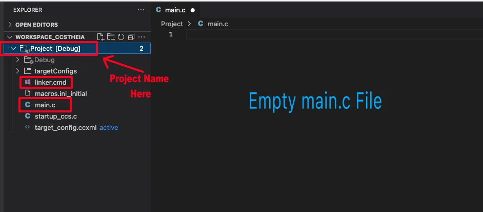
Creating and Configure a New CCS Project for Tiva C LaunchPad
I have already explained how to create a new project in TM4C123 using CCStudio. You can create a similar project with blinky template and then modify it for this tutorial.
There are only 2 things we need to do to turn the blinky template into a new project:
- Delete everything from the blinky.c file, so it should be completely empty. We will write everything ourselves.
- Rename the following:
- blinky.c → main.c, indicating that this is the main file for the project
- blinky_css.cmd → linker.cmd, indicating that this is the linker file
- blinky (Folder) → projectName (Folder)
The final modified project is shown in the image below.
After creating the project, add basic_conf.c and basic_conf.h files in the project directory. These files will configure the following:
- Configure the System to use Main Oscillator (MOSC) along with PLL to run the MCU at 80MHz. Check out the Clock Configuration in TM4C123G Tutorial.
- Configure the SysTick Timer as the timebase for delay functions. Check out TM4C123G Delay Tutorial.

- Add the
#include "basic_conf.h"to include the basic configuration library file and#include "driverlib/interrupt.h"to include interrupt functions in the main file. - Inside the main function, call
systemClockConfig()to configure the PLL to run the system at 80MHz clock. - After everything else is initialized, call
IntMasterEnable()to enable the master interrupt. This is needed for the SysTick based Delay to work.
Main Code for Testing
Here’s the complete test code:
uint8_t RxData = 0;

int main(void)
{
    systemClockConfig();
    I2C0_Init();
    IntMasterEnable();

    // Write and Read Test
    I2C_WriteByte(0x50, 0x0010, 0xAC);   // Write 0xAC to EEPROM at address 0x0010
    delay_ms(5);                         // Small delay for internal write cycle
    RxData = I2C_ReadByte(0x50, 0x0010); // Read back from the same address

    while(1)
    {
        delay_ms(1);
    }
}How the Code Works
- System and I2C Initialization
ThesystemClockConfig()sets the system clock (usually 80 MHz), andI2C0_Init()configures the I2C0 peripheral for master mode.IntMasterEnable()enables global interrupts, it is required for the sysTick timer to work. - Writing Data
The functionI2C_WriteByte(0x50, 0x0010, 0xAC)writes one byte (0xAC) to memory address0x0010in the EEPROM.
The address0x50is the 7-bit slave address of the 24C256. - Delay for Write Cycle
Thedelay_ms(5)ensures the EEPROM has enough time (typically 5 ms) to complete the internal write process before another command is issued. - Reading Data
TheI2C_ReadByte(0x50, 0x0010)function sends the same address and reads one byte from it.
The returned value is stored inRxData.
Debugging the Result
You can open the debugger watch window and add the RxData variable to Watch.
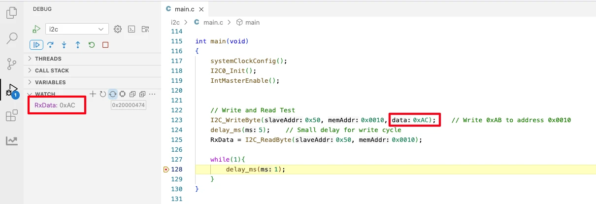
After running the code, you can see the value of the RxData variable is 0xAC. This is the value read from the EEPROM memory address 0x0010. We stored the same value at this address and now it is read back from it.
Logic Analyzer Output
To visually confirm the communication, connect a logic analyzer to the SDA and SCL lines and capture the waveform during the test.
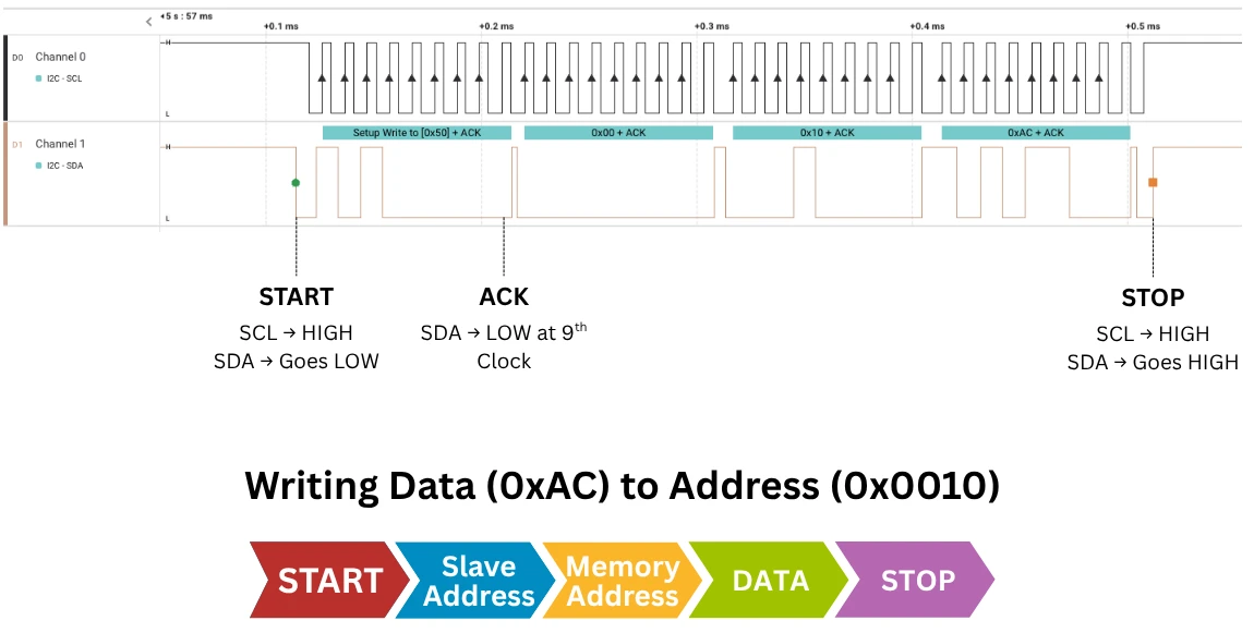
The image below shows the output of logic analyzer when the Data byte (0xAC) is written to address 0x0010. It shows the Start Condition, ACK, Data written to the slave and Stop Condition.
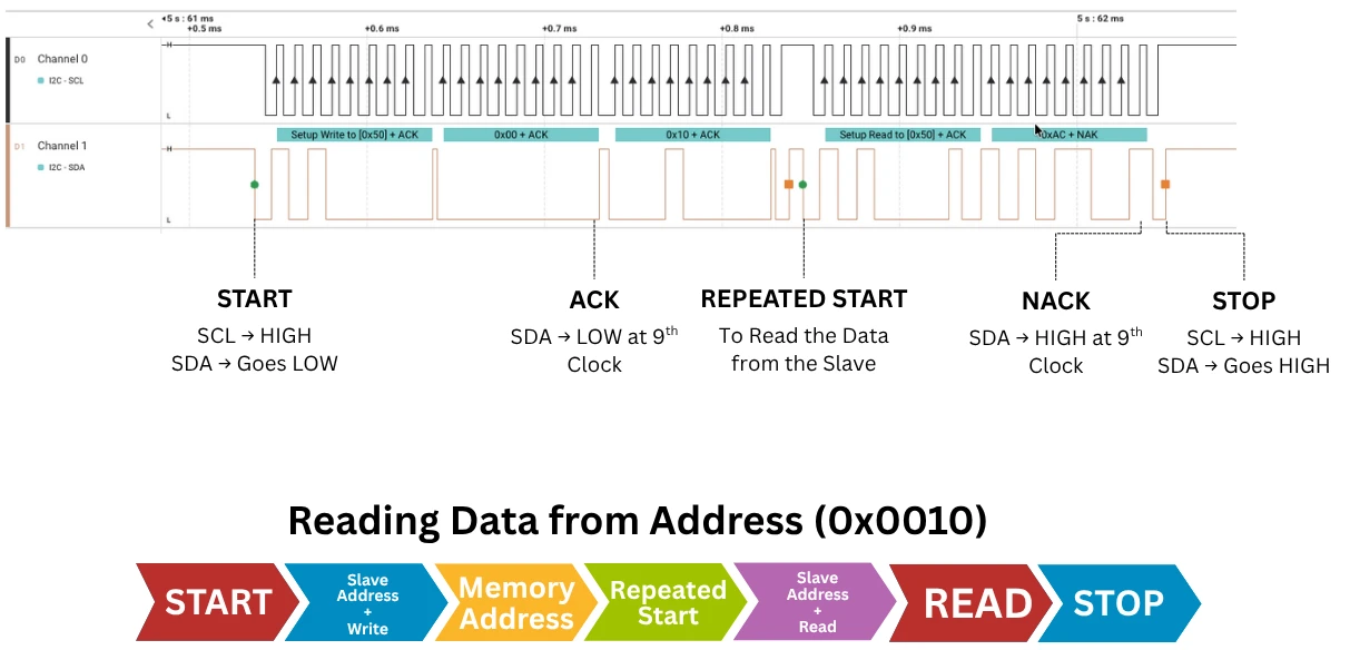
Similarly, the image below shows the output of when the Data byte is Read from address 0x0010. It shows the Start Condition, ACK, Repeated Start, Data Read from slave, Nack and the Stop Condition.
Troubleshooting I2C Communication
Even with correct setup and code, I2C communication can sometimes fail due to wiring mistakes, timing mismatches, or hardware issues. This section covers the most common I2C problems you may face when working with the TM4C123G Tiva C LaunchPad and how to fix them quickly.
Common I2C Errors and Fixes
- No Acknowledgment (NACK) from Slave
- Cause: Incorrect slave address, missing pull-up resistors, or the slave not powered.
- Fix: Double-check the 7-bit address (0x50 for 24C256) and ensure SDA/SCL lines have 4.7kΩ–10kΩ pull-ups to 3.3V. Also confirm that GND is shared between master and slave.
- Bus Stuck Low (SDA or SCL always low)
- Cause: A hung device on the bus or incorrect initialization.
- Fix: Power-cycle both the master and slave. If still stuck, reconfigure the I2C pins as GPIO and toggle SCL manually a few times to release the bus.
- Incorrect Data Read
- Cause: Reading before EEPROM completes the internal write cycle.
- Fix: Add a delay (around 5 ms) after every write, or poll the device until it responds with an ACK.
- I2C Timeout or Lockup
- Cause: Missing STOP condition or interrupted transmission.
- Fix: Ensure every transaction ends with a STOP signal. Using TivaWare’s
I2CMasterControl()commands correctly handles this automatically.
Debugging Tips for NACK and Bus Hang Issues
- Always monitor the I2CMasterBusy() flag before sending the next command.
- If you get repeated NACKs, check if the EEPROM write cycle is still in progress.
- For debugging, you can enable I2C error interrupts or read the I2CMasterErr() status to detect bus faults.
- Use a slower I2C clock speed (100 kHz) when starting out—this improves signal reliability, especially with long jumper wires.
Tip: If your code suddenly works when you connect a logic analyzer or scope probe, it’s often due to floating lines or missing pull-ups. Add proper resistors to stabilize the bus.
Checking SDA and SCL Lines on Oscilloscope
Using an oscilloscope or logic analyzer is one of the best ways to verify I2C activity:
- You should see clear square wave signals on both SCL (clock) and SDA (data) lines.
- The START condition appears when SDA goes low while SCL stays high.
- The STOP condition is when SDA goes high while SCL remains high.
- Each data bit is valid when SDA is stable while SCL is high, and an ACK appears as a low pulse on SDA after every byte.
If the signals look noisy or distorted, check for:
- Too-long wires or high capacitance on the bus.
- Weak pull-up resistors (use 4.7kΩ for 3.3V operation).
- Incorrect grounding or interference from other peripherals.
With proper signal levels and timing, you’ll get stable and error-free I2C communication every time.
Conclusion
In this tutorial, we learned how to use the I2C peripheral in TM4C123G Tiva C LaunchPad using TivaWare APIs. We explored the basics of I2C communication, understood how START, STOP, and ACK signals work, and configured the I2C0 module step by step. Using a 24C256 EEPROM, we successfully demonstrated how to write and read data over I2C, and verified the communication through the debugger and a logic analyzer.
This knowledge is extremely useful for any embedded developer working with sensors, displays, memory devices, or RTC modules, since I2C is one of the most widely used communication protocols in embedded systems. With this foundation, you can now extend the code to handle multi-byte transfers, interface with different I2C sensors, or even create your own I2C drivers for advanced applications.
Browse More TM4C123G Tutorials
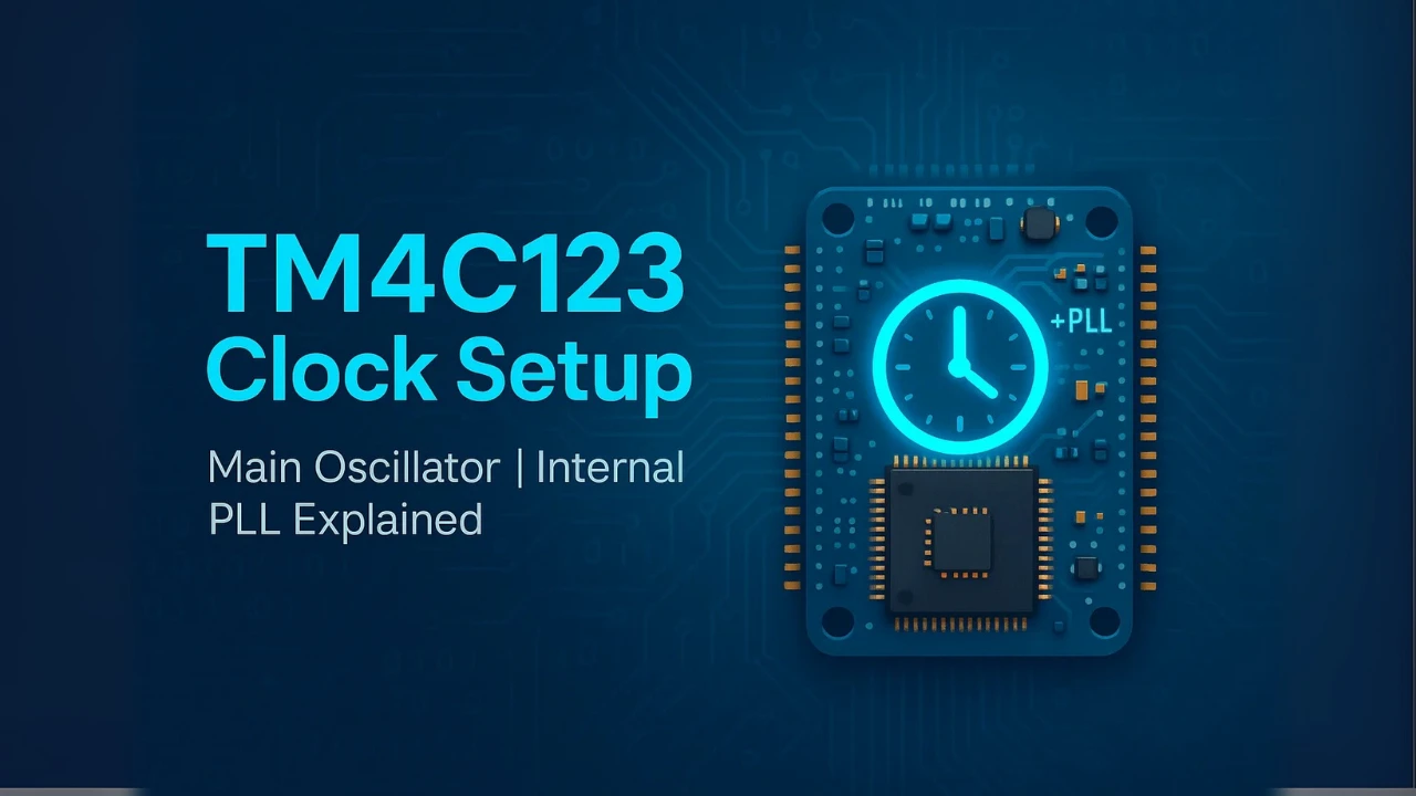
TM4C123 Clock Configuration: Main Oscillator, PIOSC & PLL with TivaWare
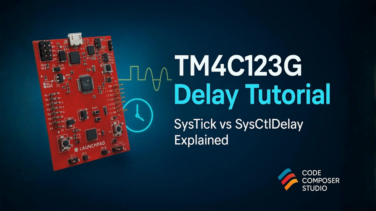
TM4C123G Delay Tutorial – Using SysCtlDelay and SysTick Timer
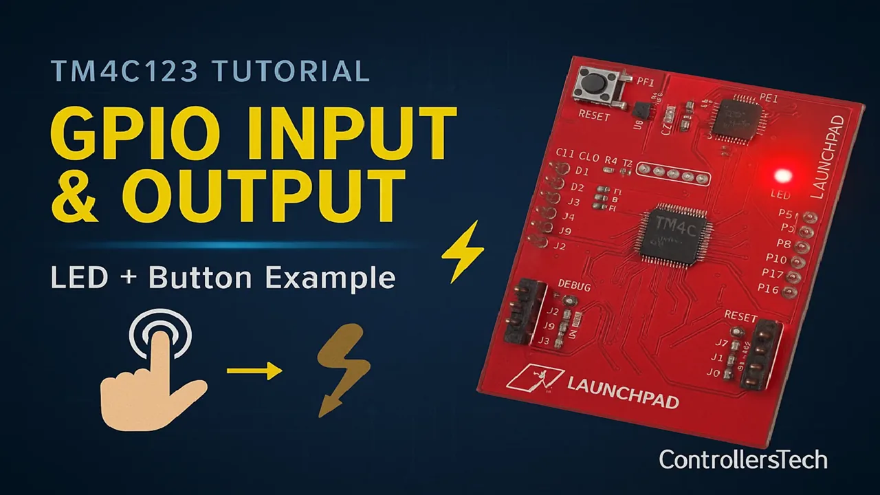
TM4C123 GPIO Tutorial – Digital Input and Output using Tiva C LaunchPad
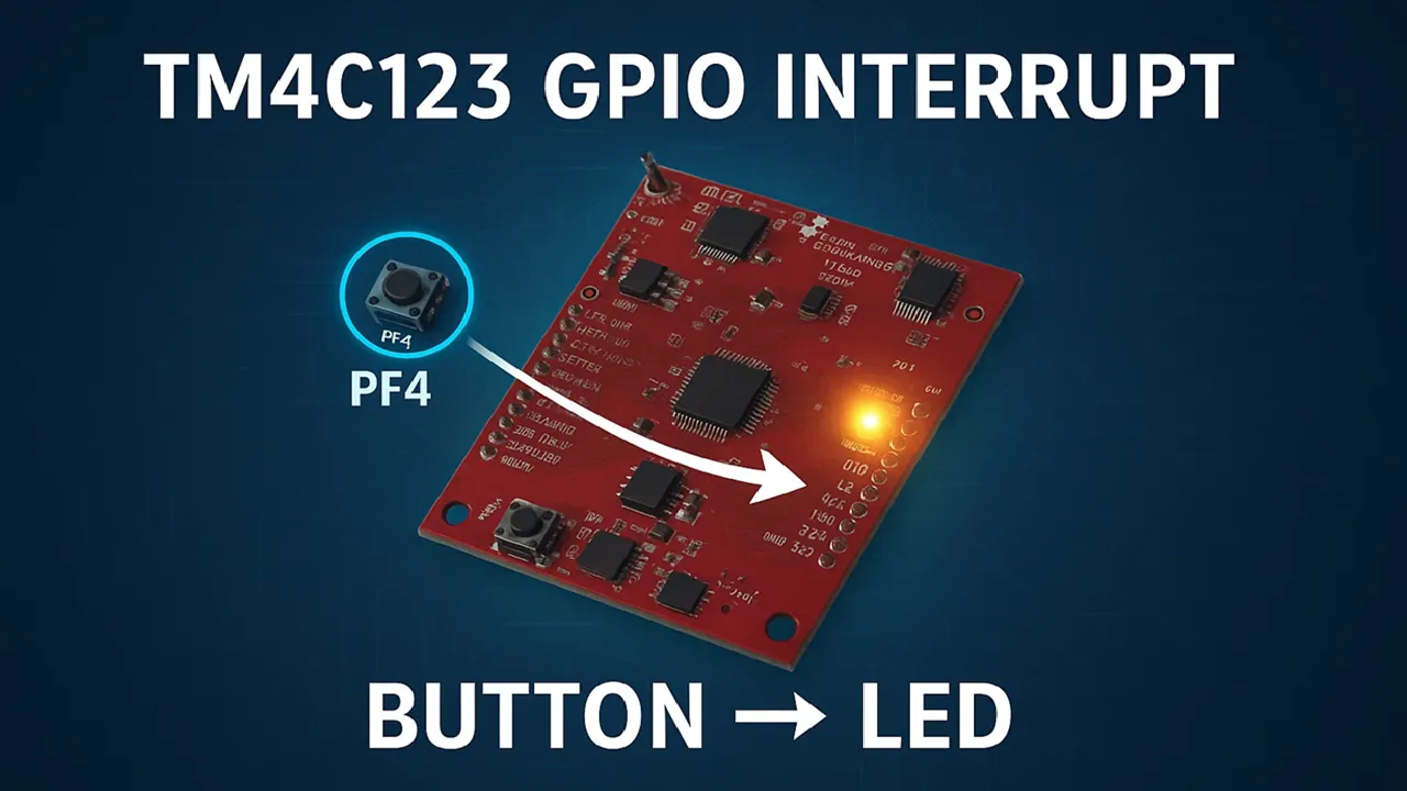
TM4C123 GPIO External Interrupts (Using TivaWare in Code Composer Studio)
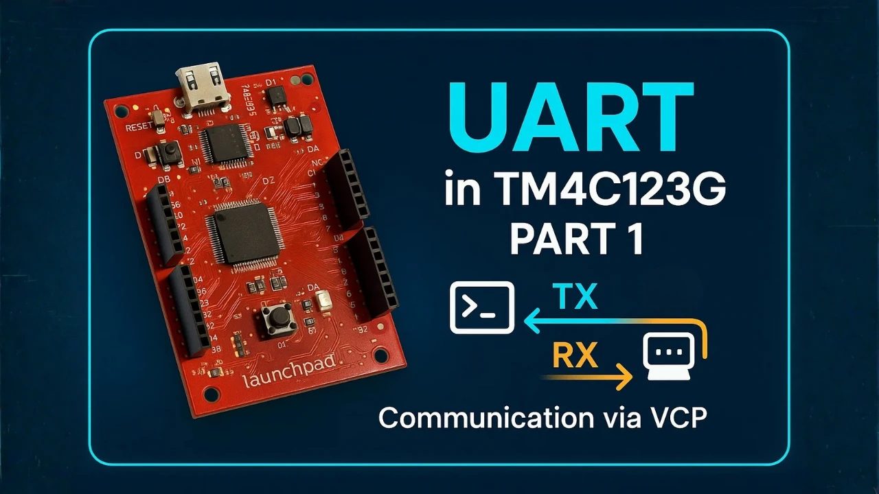
TM4C123G UART Tutorial (PART 1) – How to Use UART and Virtual COM Port in Tiva C
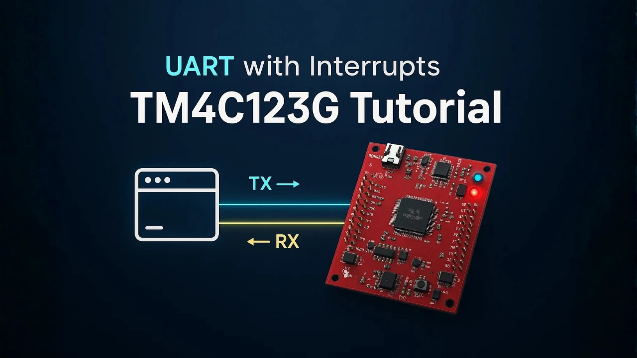
TM4C123G UART Tutorial (PART 2): Use Interrupt to Receive Data and Control LEDs
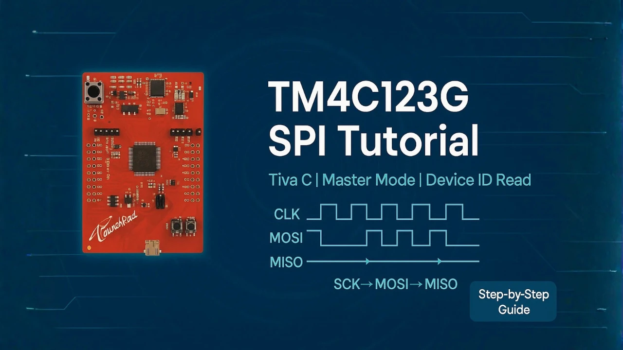
TM4C123G SPI Tutorial: Configure SSI0 & Read ADXL345 with TivaWare
TM4C123G I2C Project Download
TM4C123G I2C FAQs

Subscribe
Login
0 Comments
Newest
