Published: December 1, 2025
Last Updated: February 5, 2026
Last Updated: February 5, 2026
Interfacing Multiple ADC Channels in TM4C123G
In this tutorial, we will learn how to interface multiple ADC channels in the TM4C123G microcontroller. The TM4C123G comes with a powerful 12-bit ADC module that supports several sample sequencers, allowing us to read more than one analog signal in a single conversion cycle. This makes the ADC fast, flexible, and ideal for applications like sensor arrays, robotics, data logging, and real-time monitoring.
In this guide, we will use ADC0 Sequencer 2 to read four analog inputs connected to PE3, PE2, PE1, and PE0 (AIN0–AIN3). Sequencer 2 supports four steps, so it is a perfect match for reading four channels in one shot. We will also set up UART0 to print the ADC readings on the serial terminal.
By the end, you will know how to configure GPIO pins for analog input, set up the ADC sequencer, trigger conversions, read the results, and display them using UART. This is the fastest way to get multi-channel ADC working on the TM4C123 LaunchPad.
Prerequisite:
You should go through the previous tutorial on ADC in TM4C123G.
Introduction to TM4C123G Multiple Channel ADC
The TM4C123G microcontroller includes a flexible 12-bit ADC that supports several input channels and multiple sample sequencers. This feature makes it easy to read more than one analog signal in a single conversion cycle. In this section, we will understand how multi-channel ADC works on the TM4C123G and why Sequencer 2 is ideal for reading four analog inputs at once.
What is Multi-Channel ADC in TM4C123G?
Multi-channel ADC means the ADC module can sample several analog inputs using one ADC unit. The TM4C123G provides two ADC modules (ADC0 and ADC1), each capable of handling multiple channels through internal sample sequencers.
Instead of reading one pin at a time, the sequencer allows the ADC to convert a sequence of channels automatically. You simply configure which channel should be sampled at each step, trigger the ADC once, and then read all the results together. This saves time and increases efficiency, especially when reading sensors continuously.
Why Use Sequencer 2 for Multiple Channels?
The TM4C123G comes with four sample sequencers: SS0, SS1, SS2, and SS3.
Each sequencer supports a different number of steps:
- SS0 → 8 steps
- SS1 → 4 steps
- SS2 → 4 steps
- SS3 → 1 step
For reading four analog channels, SS2 is a perfect choice because:
- It supports exactly 4 steps, matching our requirement.
- It is simpler than SS0 and does not require extra configuration.
- It can be triggered by the processor, which makes the code easy to manage.
Using SS2 keeps the configuration clean and efficient, while still allowing us to read four samples in one ADC cycle.
Pins Used and ADC Channel Mapping
In this tutorial, we will read four analog inputs from GPIO Port E. These pins function only as ADC inputs and cannot operate as regular digital GPIO once you configure them for analog mode.
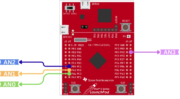
Here is the mapping:
| Pin | TM4C123G Port | ADC Channel |
|---|---|---|
| PE3 | GPIO_PORTE | AIN0 |
| PE2 | GPIO_PORTE | AIN1 |
| PE1 | GPIO_PORTE | AIN2 |
| PE0 | GPIO_PORTE | AIN3 |
These four channels map to Sequencer 2 steps 0, 1, 2, and 3, allowing you to read all of them with a single trigger. This mapping must match the hardware setup and the code configuration so that each ADC reading corresponds to the correct input pin.
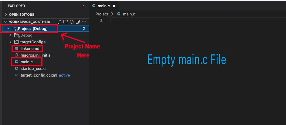
Setting up a new project in CCS
I have already explained how to create a new project in TM4C123 using CCStudio. You can create a similar project with blinky template and then modify it for this tutorial.
There are only 2 things we need to do to turn the blinky template into a new project:
- Delete everything from the blinky.c file, so it should be completely empty. We will write everything ourselves.
- Rename the following:
- blinky.c → main.c, indicating that this is the main file for the project
- blinky_css.cmd → linker.cmd, indicating that this is the linker file
- blinky (Folder) → projectName (Folder)
The final modified project is shown in the image below.
After creating the project, add basic_conf.c and basic_conf.h files in the project directory. These files will configure the following:
- Configure the System to use Main Oscillator (MOSC) along with PLL to run the MCU at 80MHz. Check out the Clock Configuration in TM4C123G Tutorial.
- Configure the SysTick Timer as the timebase for delay functions. Check out TM4C123G Delay Tutorial.

- Add the
#include "basic_conf.h"to include the basic configuration library file and#include "driverlib/interrupt.h"to include interrupt functions in the main file. - Inside the main function, call
systemClockConfig()to configure the PLL to run the system at 80MHz clock. - After everything else is initialized, call
IntMasterEnable()to enable the master interrupt. This is needed for the SysTick based Delay to work.
Initializing UART0 Initialization for Debug printf
UART0 is used in this project to print debug messages. This helps us confirm whether the project is working correctly. The UART0 is connected to the Virtual COM Port (VCP) through the on-board debugger, so no external hardware is required to view the output.
You can check more information about UART on the Tiva C LaunchPad by visiting the following link:
Use UART VCP in TiVa C.
The function below sets up UART0 on pins PA0 (RX) and PA1 (TX) at a baud rate of 115200.
#include "driverlib/uart.h"
#include "utils/uartstdio.h"
void UART0_Init(void)
{
    SysCtlPeripheralEnable(SYSCTL_PERIPH_UART0);
    SysCtlPeripheralEnable(SYSCTL_PERIPH_GPIOA);

    GPIOPinConfigure(GPIO_PA0_U0RX);
    GPIOPinConfigure(GPIO_PA1_U0TX);
    GPIOPinTypeUART(GPIO_PORTA_BASE, GPIO_PIN_0 | GPIO_PIN_1);

    UARTClockSourceSet(UART0_BASE, UART_CLOCK_PIOSC);

    UARTStdioConfig(0, 115200, 16000000);
}Explanation
- Enable UART0 and GPIOA clocks.
Required before configuring any pins or UART registers. - Configure PA0 and PA1 for UART.
PA0: U0RX, PA1: U0TX using alternate pin functions. - Set pin type to UART.
Activates UART electrical characteristics on these pins. - Select UART clock source.
Uses the 16 MHz PIOSC for stable baud rate generation. - Configure UARTStdio.
Sets baud rate to 115200 and preparesUARTprintf()for debugging.
Important Note
To use UARTprintf() and UARTStdioConfig(), you must add the file to your project:
TivaWare/utils/uartstdio.cCreate a folder named utils inside your project and copy uartstdio.c into it.
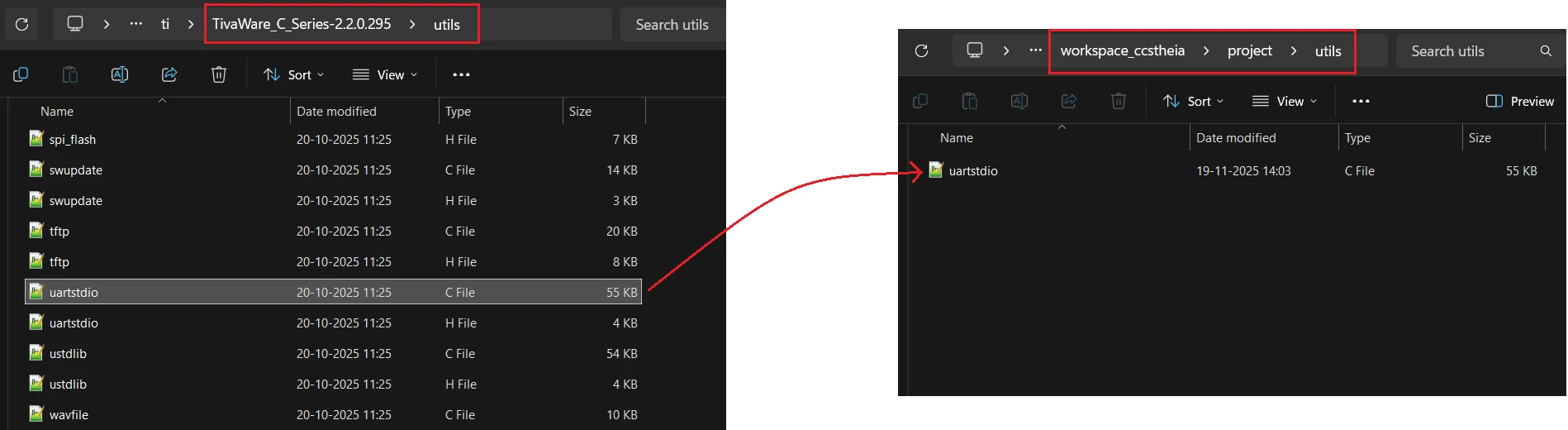
Without this file, the linker will give errors for undefined symbols.
Configuring ADC0 for Reading Multiple Channels
To read four analog channels from Port E, we must enable the required peripherals, configure the pins as analog inputs, set up the ADC sequencer, and assign one channel to each sequencer step.
The steps are simple and follow the same flow as your previous ADC tutorial.
Enabling ADC0 and GPIOE Peripheral Clocks
Before using the ADC, you must enable the clocks for both ADC0 and GPIOE. GPIOE is needed because all four analog inputs (PE3–PE0) are located on this port.
Below is the code to enable ADC0 and GPIOE:
// Enable ADC0 and GPIOE clocks
SysCtlPeripheralEnable(SYSCTL_PERIPH_ADC0);
SysCtlPeripheralEnable(SYSCTL_PERIPH_GPIOE);

// Wait until peripherals are ready
while(!SysCtlPeripheralReady(SYSCTL_PERIPH_ADC0));
while(!SysCtlPeripheralReady(SYSCTL_PERIPH_GPIOE));This ensures both modules are powered and ready before you configure them.
Configuring PE3–PE0 as Analog Inputs
The pins PE3, PE2, PE1, and PE0 correspond to ADC channels AIN0, AIN1, AIN2, and AIN3.
To use these pins as analog inputs:
- Disable the digital functions on these pins.
- TivaWare automatically configures the pins for analog mode.
- You don’t need to apply any alternate-function settings for ADC inputs.
Below is the code to configure these pins:
// Configure PE3-PE0 as ADC inputs (AIN0-AIN3)
GPIOPinTypeADC(GPIO_PORTE_BASE, GPIO_PIN_3 | GPIO_PIN_2 | GPIO_PIN_1 | GPIO_PIN_0);TivaWare automatically takes care of internal digital disable and analog enable.
Disabling and Configuring ADC Sample Sequencer 2
TM4C123G has four sequencers: SS0, SS1, SS2, and SS3. Sequencer SS2 supports exactly 4 steps, so it is perfect for sampling four ADC channels in one trigger.
We configure SS2 to:
- Use processor trigger (software controlled)
- Use priority 0 (highest priority)
Below is the code:
// Disable SS2 before configuration
ADCSequenceDisable(ADC0_BASE, 2);

// Configure SS2 for processor trigger, highest priority
ADCSequenceConfigure(ADC0_BASE, 2, ADC_TRIGGER_PROCESSOR, 0);This sets up the sequencer for multi-channel sampling.
Assigning ADC Channels to Each Sequencer Step
Sequencer 2 supports four conversion steps.
We assign channels as:
| Step | Pin | ADC Channel |
|---|---|---|
| 0 | PE3 | AIN0 |
| 1 | PE2 | AIN1 |
| 2 | PE1 | AIN2 |
| 3 | PE0 | AIN3 + END |
The last step must contain ADC_CTL_END to mark conversion completion.
Below is the code:
// Configure step 0 to sample AIN0
ADCSequenceStepConfigure(ADC0_BASE, 2, 0, ADC_CTL_CH0);

// Configure step 1 to sample AIN1
ADCSequenceStepConfigure(ADC0_BASE, 2, 1, ADC_CTL_CH1);

// Configure step 2 to sample AIN2
ADCSequenceStepConfigure(ADC0_BASE, 2, 2, ADC_CTL_CH2);

// Configure step 3 to sample AIN3 (with END flag)
ADCSequenceStepConfigure(ADC0_BASE, 2, 3, ADC_CTL_CH3 | ADC_CTL_END);Enabling Sequencer 2
After all steps are configured, we re-enable SS2:
// Enable Sequencer 2
ADCSequenceEnable(ADC0_BASE, 2);The ADC is now fully configured for multi-channel sampling.
Complete ADC Configuration Code
void ADC0_Init(void)
{
    // 1. Enable ADC0 and GPIOE clocks
    SysCtlPeripheralEnable(SYSCTL_PERIPH_ADC0);
    SysCtlPeripheralEnable(SYSCTL_PERIPH_GPIOE);

    while(!SysCtlPeripheralReady(SYSCTL_PERIPH_ADC0));
    while(!SysCtlPeripheralReady(SYSCTL_PERIPH_GPIOE));

    // 2. Configure PE3-PE0 as analog inputs
    GPIOPinTypeADC(GPIO_PORTE_BASE, GPIO_PIN_3 | GPIO_PIN_2 | GPIO_PIN_1 | GPIO_PIN_0);

    // 3. Configure ADC0 Sequencer 2
    ADCSequenceDisable(ADC0_BASE, 2);
    ADCSequenceConfigure(ADC0_BASE, 2, ADC_TRIGGER_PROCESSOR, 0);

    // 4. Set channels for each step
    ADCSequenceStepConfigure(ADC0_BASE, 2, 0, ADC_CTL_CH0);
    ADCSequenceStepConfigure(ADC0_BASE, 2, 1, ADC_CTL_CH1);
    ADCSequenceStepConfigure(ADC0_BASE, 2, 2, ADC_CTL_CH2);
    ADCSequenceStepConfigure(ADC0_BASE, 2, 3, ADC_CTL_CH3 | ADC_CTL_END);

    // 5. Enable Sequencer 2
    ADCSequenceEnable(ADC0_BASE, 2);
}Reading ADC Data From All Channels
Once you configure the ADC sequencer, you trigger conversions and read the samples it generates. If you’re using ADC Sequencer 2 (SS2) with four steps, the ADC can read four channels in one sequence.
In this section, we will trigger the ADC manually, wait for the conversion to finish, and then read all four samples into a buffer.
Triggering ADC Conversion Using Processor Trigger
To start an ADC conversion through software, we use the processor trigger. This forces the ADC to begin sampling immediately.
Below is the code to start the ADC sampling:
// Start ADC conversion using processor trigger
ADCProcessorTrigger(ADC0_BASE, 2);Here:
ADC0_BASE: ADC0 module2: Sequencer 2 (SS2)
Reading Four Samples Using ADCSequenceDataGet
Each step in Sequencer 2 stores one sample. If you configured SS2 with four steps, you get four ADC results.
Below is the code to read all ADC samples into an array:
uint32_t array[4];   // Array for 4 samples

// Read all samples from SS0
ADCSequenceDataGet(ADC0_BASE, 2, array);Now:
array[0]-> sample from step 0array[1]-> sample from step 1array[2]-> sample from step 2array[3]-> sample from step 3
These values range from 0 to 4095 for 12-bit resolution.
Full Example: Reading 4 ADC Channels Using SS2
Here is the complete code for the reading part only, assuming your ADC and SS2 are already configured:
uint32_t array[4];
void ADC0_Read(uint32_t *array)
{
    // Trigger SS2 conversion
    ADCProcessorTrigger(ADC0_BASE, 2);

    // Read the ADC value
    ADCSequenceDataGet(ADC0_BASE, 2, array);
}Printing ADC Values on UART
Once all four ADC channels are sampled, the next step is to print them on the UART terminal. This helps you verify the readings in real time and makes debugging much easier. In this section, we will loop through the ADC results, convert each value into a readable string, and finally send the formatted data over UART using UARTprintf().
Looping Through the ADC Result Array
After calling the ADC read function, the four samples are stored in an array. Each index corresponds to one ADC input channel.
Here is how we loop through all four values:
while(1)
{
   ADC0_Read(adcVal);
   int i=0;
   for (i=0; i<4; i++){
       UARTprintf("CH%d: %u\t", i, adcVal[i]);
   }
   UARTprintf("\n");
   delay_ms(200);
}This simple loop reads the 4 ADC channels and prints all channels in a single line.
After conversion, each value is sent to the UART terminal using UARTprintf().
Example:
UARTprintf("CH%d: %u\t", i, adcVal[i]);This prints:
CH0: 1023 CH1: 980 CH2: 750 CH3: 512A newline is added after every loop so the next reading starts on a new line:
UARTprintf("\n");This gives you clean and readable output in the serial terminal.
Complete Code for TM4C123G Multiple Channel ADC
In this section, we will combine everything into one working program. The full source code includes system clock configuration, UART setup, ADC initialization, and reading four ADC channels using Sequencer 2. After each conversion, the ADC values are printed on the UART terminal in a clear and simple format.
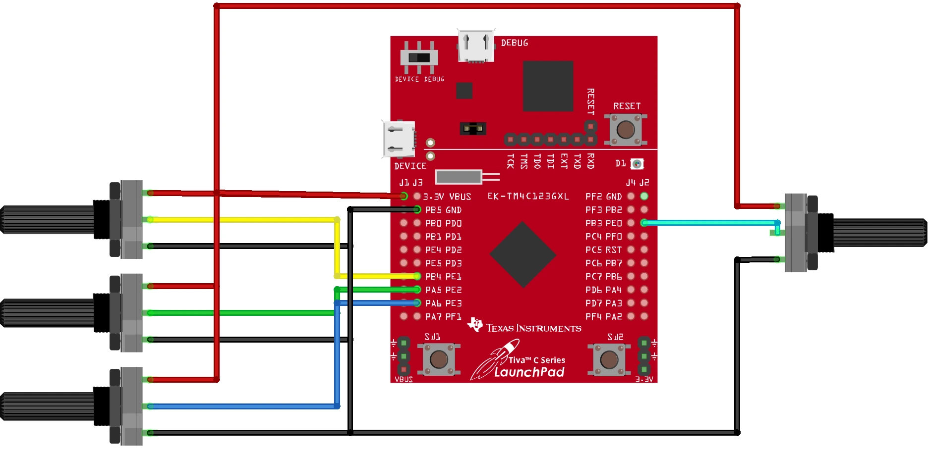
Wiring Diagram
The image below shows the 4 potentiometers connected to the 4 channels of ADC0 in TM4C123G dev board.
Full Source Code
Below is the complete code exactly as used in this tutorial. You can copy and run it directly on the TM4C123G LaunchPad.
//*****************************************************************************
// TM4C123G - Multiple Channel ADC using Sequencer 2
//*****************************************************************************

#include <stdint.h>
#include <stdbool.h>
#include "inc/hw_memmap.h"
#include "driverlib/pin_map.h"
#include "driverlib/gpio.h"
#include "driverlib/sysctl.h"
#include "driverlib/interrupt.h"
#include "basic_conf.h"
#include "driverlib/adc.h"

#include "driverlib/uart.h"
#include "utils/uartstdio.h"

// UART0 Initialization
void UART0_Init(void)
{
    SysCtlPeripheralEnable(SYSCTL_PERIPH_UART0);
    SysCtlPeripheralEnable(SYSCTL_PERIPH_GPIOA);

    GPIOPinConfigure(GPIO_PA0_U0RX);
    GPIOPinConfigure(GPIO_PA1_U0TX);
    GPIOPinTypeUART(GPIO_PORTA_BASE, GPIO_PIN_0 | GPIO_PIN_1);

    UARTClockSourceSet(UART0_BASE, UART_CLOCK_PIOSC);

    UARTStdioConfig(0, 115200, 16000000);
}

// ADC0 Initialization for 4 Channels Using Sequencer 2
void ADC0_Init(void)
{
    // Enable ADC0 and GPIOE
    SysCtlPeripheralEnable(SYSCTL_PERIPH_ADC0);
    SysCtlPeripheralEnable(SYSCTL_PERIPH_GPIOE);

    while(!SysCtlPeripheralReady(SYSCTL_PERIPH_ADC0));
    while(!SysCtlPeripheralReady(SYSCTL_PERIPH_GPIOE));

    // Configure PE3, PE2, PE1 & PE0 as analog inputs
    GPIOPinTypeADC(GPIO_PORTE_BASE,
                   GPIO_PIN_3 | GPIO_PIN_2 | GPIO_PIN_1 | GPIO_PIN_0);

    // Disable SS2 before configuration
    ADCSequenceDisable(ADC0_BASE, 2);

    // Configure SS2 for processor trigger
    ADCSequenceConfigure(ADC0_BASE, 2, ADC_TRIGGER_PROCESSOR, 0);

    // Configure steps for channels AIN0, AIN1, AIN2, AIN3
    ADCSequenceStepConfigure(ADC0_BASE, 2, 0, ADC_CTL_CH0);
    ADCSequenceStepConfigure(ADC0_BASE, 2, 1, ADC_CTL_CH1);
    ADCSequenceStepConfigure(ADC0_BASE, 2, 2, ADC_CTL_CH2);
    ADCSequenceStepConfigure(ADC0_BASE, 2, 3, ADC_CTL_CH3 | ADC_CTL_END);

    // Enable SS2
    ADCSequenceEnable(ADC0_BASE, 2);
}

// Read 4 Samples from Sequencer 2
void ADC0_Read(uint32_t *array)
{
    // Trigger SS2 conversion
    ADCProcessorTrigger(ADC0_BASE, 2);

    // Fetch 4 ADC samples
    ADCSequenceDataGet(ADC0_BASE, 2, array);
}

uint32_t adcVal[4];

int main(void)
{
    systemClockConfig();
    UART0_Init();
    ADC0_Init();
    IntMasterEnable();

    while(1)
    {
        ADC0_Read(adcVal);

        for (int i = 0; i < 4; i++)
        {
            UARTprintf("CH%d: %u\t", i, adcVal[i]);
        }

        UARTprintf("\n");
        delay_ms(200);
    }
}How the Code Works:
Here is a simple breakdown of how this program works:
1. System Clock and UART Setup
The clock is configured first, then UART0 is initialized on PA0 (RX) and PA1 (TX).
UART is set to 115200 baud, which is ideal for debugging.
2. Enabling ADC0 and Configuring GPIOE
ADC0 and GPIOE clocks are enabled.
Pins PE0–PE3 are set as analog inputs.
These correspond to AIN0, AIN1, AIN2, AIN3.
3. Setting Up Sequencer 2
Sequencer 2 (SS2) supports 4 steps, so it can read four channels in one trigger.
Steps configured:
| SS2 Step | ADC Channel | Pin |
|---|---|---|
| 0 | AIN0 | PE3 |
| 1 | AIN1 | PE2 |
| 2 | AIN2 | PE1 |
| 3 | AIN3 | PE0 |
The last step uses ADC_CTL_END to mark the end of sequence.
4. Triggering the ADC
When ADCProcessorTrigger() runs, all four steps of SS2 are sampled instantly.
5. Reading All 4 Values
ADCSequenceDataGet() fills the array with:
array[0] -> Sample from AIN0
array[1] -> Sample from AIN1
array[2] -> Sample from AIN2
array[3] -> Sample from AIN36. Printing Results on UART
Each sample is printed using:
UARTprintf("CH%d: %u\t", i, adcVal[i]);This makes checking ADC readings very easy.
Output on UART Terminal
When the program runs, you will see output like this (video below) on the UART terminal (115200 baud):
Each line represents the four ADC channels sampled in one sequence:
- CH0 -> AIN0 (PE3)
- CH1 -> AIN1 (PE2)
- CH2 -> AIN2 (PE1)
- CH3 -> AIN3 (PE0)
The readings update every 200 ms.
Conclusion
In this tutorial, we walked through the complete process of configuring the TM4C123G’s ADC to read analog inputs from multiple channels and display the results over UART. Starting from enabling the required peripherals, setting up UART0 for debugging, and configuring the ADC sequence, we built a reliable foundation for capturing sensor data. You also learned how the processor trigger is used to start conversions, how the raw values are retrieved, and how those results are prepared for output.
By combining ADC sampling with UART printing, you now have a powerful diagnostic setup suitable for real-time monitoring, sensor testing, and embedded debugging. This workflow is extremely useful in projects involving environmental sensors, voltage measurements, robotics control, or any application that needs immediate feedback from analog inputs. With this structure in place, you can easily expand the code to support more channels, add filtering, or stream data to a PC or logging system for deeper analysis.
Browse More TM4C123G Tutorials
TM4C123G Clock Setup Tutorial – Configure System Clock with PLL
TM4C123G Delay Tutorial – Using SysCtlDelay and SysTick Timer
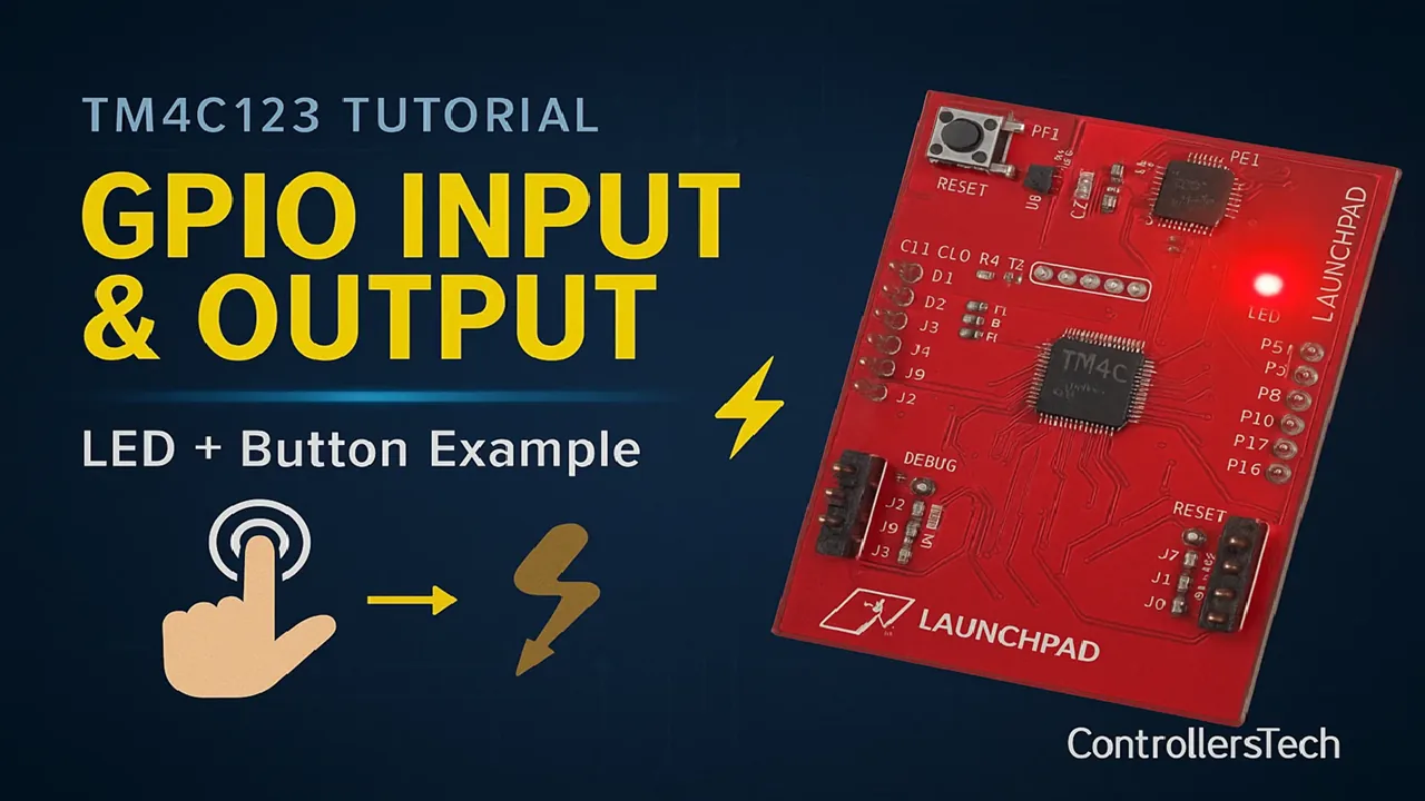
TM4C123 GPIO Tutorial – Digital Input and Output using Tiva C LaunchPad
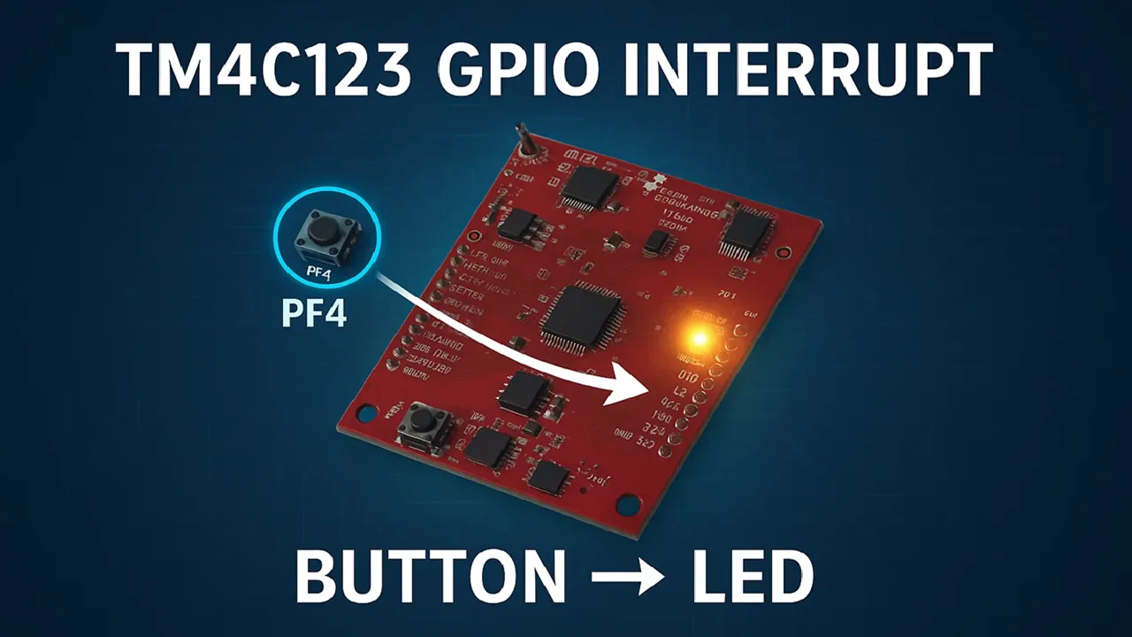
TM4C123 GPIO External Interrupts (Using TivaWare in Code Composer Studio)
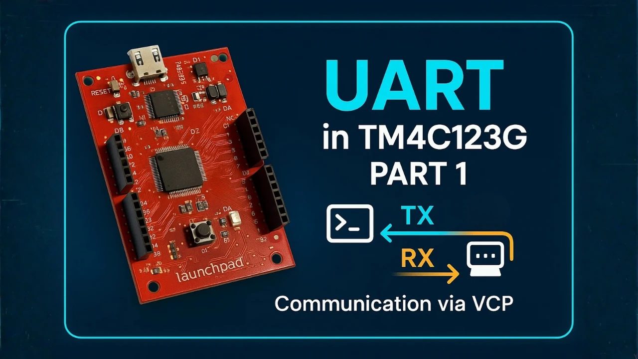
TM4C123G UART Tutorial (PART 1) – How to Use UART and Virtual COM Port in Tiva C
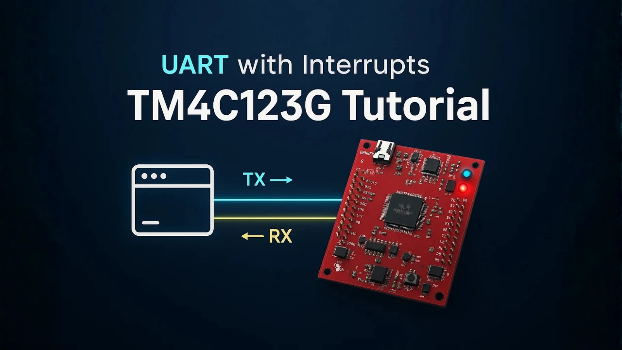
TM4C123G UART Tutorial (PART 2): Use Interrupt to Receive Data and Control LEDs
I2C in TM4C123G Tiva C – How to Use I2C Peripheral with TivaWare
TM4C123G MultiADC Project Download
TM4C123G ADC FAQs
Subscribe
Login
0 Comments
Newest
