Last Updated: February 5, 2026
TM4C123G ADC Tutorial: Simple Guide to Configure and Read ADC Values
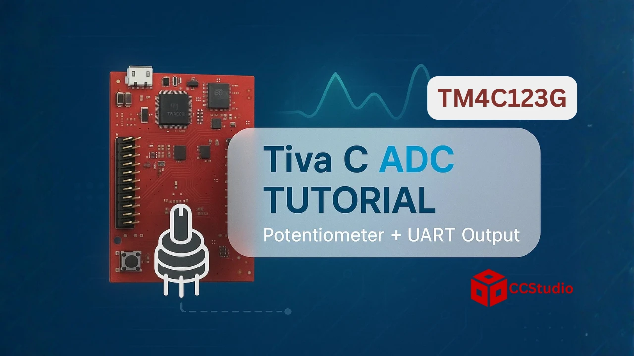
Working with analog sensors is one of the first steps when learning embedded systems. The TM4C123G LaunchPad makes this task simple with its powerful 12-bit ADC module. Whether you want to read a potentiometer, monitor temperature, or measure light intensity, the ADC lets your microcontroller understand real-world analog signals and convert them into digital values.
In this guide, we will walk through the complete process of using the ADC on the TM4C123G. You will learn how the ADC works, how to choose the right input pin, and how to configure the ADC module step-by-step. We will write clean and simple C code, explain each line in small sections, and make the output visible on the serial monitor.
The goal of this tutorial is to keep things simple and clear. Every section is short. Every explanation is easy to understand. Even beginners will be able to follow the steps without confusion.
By the end of this tutorial, you will know how to:
- Initialize the ADC peripheral correctly
- Read ADC samples from any analog pin
- Convert the ADC reading into a real voltage
- Display the result on the serial monitor through UART
This makes the TM4C123G ADC perfect for projects like sensor data logging, real-time monitoring, and learning embedded programming.
Understanding the ADC on TM4C123G
Before writing any code, it is important to understand how the ADC block works on the TM4C123G microcontroller. This section explains the basic idea behind ADCs, the features offered by the TM4C123G, and the key concepts you must know before initialization. With this knowledge, setting up and using the ADC becomes much easier.
What Is ADC and Why We Use It
ADC stands for Analog-to-Digital Converter. It converts real-world analog signals, such as voltage from sensors, into digital numbers that the microcontroller can process.
For example:
- A potentiometer outputs a varying voltage.
- An LDR changes resistance with light.
- A temperature sensor changes voltage based on temperature.
The microcontroller cannot understand these continuous analog values directly. The ADC takes the analog input and converts it into a number between 0 and 4095 (for 12-bit resolution).
This digital number represents the voltage level.
Key ADC Features in TM4C123G
The TM4C123G LaunchPad includes a powerful ADC module with many useful features.
Here are the most important ones:
- Two independent ADC modules (ADC0 and ADC1)
- 12-bit resolution, giving values from 0 to 4095
- Up to 1 million samples per second (1 MSPS)
- Four sequencers (SS0–SS3) for flexible sampling
- Support for single-ended and differential inputs
- Hardware oversampling for stable readings
- Up to 12 analog input channels (AIN0–AIN11)
- Programmable trigger sources (processor, timer, PWM, comparator, GPIO, etc.)
These features make the ADC very flexible. You can read a single sample, multiple samples, or even trigger conversions automatically using timers or interrupts.
ADC Clock, Sampling Speed and Resolution
The ADC module needs a stable clock to work correctly. On the TM4C123G, the ADC clock typically comes from the PLL or the system clock.
A few important points:
- The ADC operates best when its internal clock is 125 kHz to 16 MHz.
- The TM4C123G can sample up to 1 MSPS (1 million samples per second).
- It uses a 12-bit resolution, which means:
- 0 = 0V
- 4095 = maximum reference voltage (usually 3.3V)
The formula to convert ADC reading to voltage is:
Voltage = (ADC_Value / 4095.0) * 3.3The higher the resolution, the more precise the reading. With 12 bits, you get 4096 possible values (2^12), giving good accuracy for sensor applications.
Understanding ADC Sequencers (SS0–SS3)
The ADC on the TM4C123G uses four sequencers. Each sequencer decides how many samples to take and from which channels.
Here is the summary:
| Sequencer | Number of Samples | Priority | Common Use |
|---|---|---|---|
| SS0 | Up to 8 samples / steps | Lowest | Multi-sensor sampling |
| SS1 | Up to 4 samples / steps | Medium | Small sensor arrays |
| SS2 | Up to 4 samples / steps | Medium | Regular ADC tasks |
| SS3 | 1 sample / step | Highest | Simple, single-channel sampling |
SS3 is the most commonly used sequencer because:
- It is simple
- It takes only one sample
- It has the highest priority
- Ideal for reading a single sensor like a potentiometer
Each sequencer can be triggered by:
- Software (processor)
- Timers
- PWM
- GPIO events
- Comparators
This makes the ADC module very flexible and powerful.
Hardware Setup for TM4C123G ADC
Before writing any code, we must prepare the hardware. The TM4C123G LaunchPad does not include a built-in potentiometer, so you must use an external analog sensor or an external potentiometer. This section explains the required components, supported ADC pins, and how to wire them safely.
Using External Potentiometer or Analog Sensors
Since the TM4C123G LaunchPad has no onboard potentiometer, you need an external analog input source. A simple 10k potentiometer is the best option for testing, because it provides a clean and adjustable voltage between 0 and 3.3V.
You can also use other analog sensors, such as:
- LM35 temperature sensor
- Light sensor (LDR with a voltage divider)
- Soil moisture sensor
- Analog joystick
- Any sensor with a 0–3.3V output
These devices make it easy to test how the ADC reads varying voltages.
ADC Input Pins and Voltage Limits
The TM4C123G provides 12 analog channels, mapped to specific GPIO pins. Some commonly used pins include:
| ADC Channel | GPIO Pin |
|---|---|
| AIN0 | PE3 |
| AIN1 | PE2 |
| AIN2 | PE1 |
| AIN3 | PE0 |
| AIN8 | PE5 |
| AIN9 | PE4 |
| AIN10 | PB4 |
| AIN11 | PB5 |
The most convenient pins for beginners are PE3 (AIN0) and PE4 (AIN9) because they are easy to access on the LaunchPad header.
Voltage Limits (Important)
The ADC input must stay within:
- 0V minimum
- 3.3V maximum
Applying more than 3.3V can permanently damage the pin. If your sensor outputs 5V, use a voltage divider or level shifter.
Wiring the Sensor to the ADC Pin
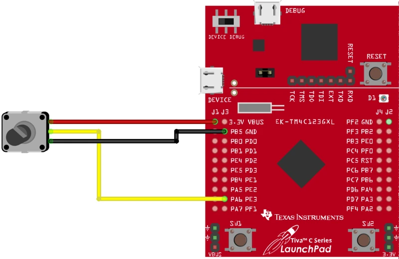
To test the ADC with a potentiometer, connect it as shown in the image below.
This setup works with any analog sensor that outputs 0–3.3V. The table below explains the pin connections.
| Potentiometer Pin | Connect To | Description |
|---|---|---|
| Left Pin | GND | Sets the lower voltage reference (0V) |
| Right Pin | 3.3V | Sets the upper voltage reference (maximum ADC voltage) |
| Middle Pin | ADC Input Pin (e.g., PE3 / AIN0) | Outputs a variable voltage based on knob position |
Setting up a new project in CCS
I have already explained how to create a new project in TM4C123 using CCStudio. You can create a similar project with blinky template and then modify it for this tutorial.
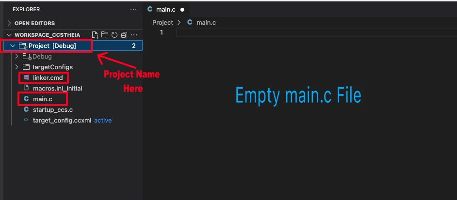
There are only 2 things we need to do to turn the blinky template into a new project:
- Delete everything from the blinky.c file, so it should be completely empty. We will write everything ourselves.
- Rename the following:
- blinky.c → main.c, indicating that this is the main file for the project
- blinky_css.cmd → linker.cmd, indicating that this is the linker file
- blinky (Folder) → projectName (Folder)
The final modified project is shown in the image below.
After creating the project, add basic_conf.c and basic_conf.h files in the project directory. These files will configure the following:
- Configure the System to use Main Oscillator (MOSC) along with PLL to run the MCU at 80MHz. Check out the Clock Configuration in TM4C123G Tutorial.
- Configure the SysTick Timer as the timebase for delay functions. Check out TM4C123G Delay Tutorial.
- Add the
#include "basic_conf.h"to include the basic configuration library file and#include "driverlib/interrupt.h"to include interrupt functions in the main file. - Inside the main function, call
systemClockConfig()to configure the PLL to run the system at 80MHz clock. - After everything else is initialized, call
IntMasterEnable()to enable the master interrupt. This is needed for the SysTick based Delay to work.
Step-By-Step ADC Initialization in TM4C123G
This section explains every ADC configuration step in simple words.
You will learn how to:
- Enable ADC and GPIO clocks
- Configure a GPIO pin for analog input
- Choose an ADC sequencer
- Select the trigger source
- Set the channel and sample control
- Finalize the ADC setup
All steps use TivaWare functions, making the code cleaner and easier to understand.
Enabling ADC and GPIO Peripheral Clock
Before using ADC, you must enable its clock and the clock for the GPIO port where your analog input pin is located. For example, if you want to read from PE3 (AIN0), both ADC0 and GPIOE must be enabled.
Below is the Code to enable ADC0 and GPIOE Clocks.
// Enable ADC0 and GPIOE clocks
SysCtlPeripheralEnable(SYSCTL_PERIPH_ADC0);
SysCtlPeripheralEnable(SYSCTL_PERIPH_GPIOE);

// Wait until peripherals are ready
while(!SysCtlPeripheralReady(SYSCTL_PERIPH_ADC0));
while(!SysCtlPeripheralReady(SYSCTL_PERIPH_GPIOE));Configuring the ADC Input Pin as Analog
ADC pins must be configured as analog inputs.
This means:
- Disable digital function
- Enable analog mode
- Keep alternate functions disabled (TivaWare handles this automatically)
Below is the code to configure PE3 as ADC Input
// Configure PE3 as an ADC input (AIN0)
GPIOPinTypeADC(GPIO_PORTE_BASE, GPIO_PIN_3);TivaWare internally handles analog mode and disables digital functionality.
Selecting ADC Sequencer and Trigger Source
TM4C123G has four sequencers (SS0–SS3).
For simple single-channel sampling, Sequencer 3 (SS3) is best because:
- It samples only one channel
- It is easy to configure
- Good for beginners
Trigger source:
We use processor trigger, meaning the software will start sampling.
Below is the code to configure the ADC sequencer, trigger source and priority.
// Disable SS3 before configuration
ADCSequenceDisable(ADC0_BASE, 3);

// Configure SS3 for processor trigger, highest priority
ADCSequenceConfigure(ADC0_BASE, 3, ADC_TRIGGER_PROCESSOR, 0);Setting Sample Control and Input Channel
Now we tell the ADC:
- Which channel to read (AIN0 : PE3)
- Whether this is the end of the sequence
- Whether to generate an interrupt (optional)
Below is the code to set the sample control and ADC channel.
// Configure SS3 step 0 to read AIN0
// ADC_CTL_END marks the end of the sequence
ADCSequenceStepConfigure(ADC0_BASE, 3, 0, ADC_CTL_CH0 | ADC_CTL_END);If you want interrupts later, you may add ADC_CTL_IE.
Finalizing the ADC Setup
Once the sequencer, steps, and channel are set:
- Enable the sequencer
- ADC is ready to sample
Below is the code to enable the sequencer.
ADCSequenceEnable(ADC0_BASE, 3); // Enable SS3ADC is now fully configured.
Final Combined ADC Initialization Code
Here is the complete setup code to initialize the ADC0 Channel 0, combining all sections:
void ADC0_Init(void)
{
    //
    // 1. Enable ADC0 and GPIOE clocks
    //
    SysCtlPeripheralEnable(SYSCTL_PERIPH_ADC0);
    SysCtlPeripheralEnable(SYSCTL_PERIPH_GPIOE);

    while(!SysCtlPeripheralReady(SYSCTL_PERIPH_ADC0));
    while(!SysCtlPeripheralReady(SYSCTL_PERIPH_GPIOE));

    //
    // 2. Configure PE3 (AIN0) as analog input
    //
    GPIOPinTypeADC(GPIO_PORTE_BASE, GPIO_PIN_3);

    //
    // 3. Configure ADC0 Sequencer 3 for processor trigger
    //
    ADCSequenceDisable(ADC0_BASE, 3);  // Disable SS3 before config
    ADCSequenceConfigure(ADC0_BASE, 3, ADC_TRIGGER_PROCESSOR, 0);

    //
    // 4. Configure step 0 of SS3 to sample AIN0
    //
    ADCSequenceStepConfigure(ADC0_BASE, 3, 0,
                             ADC_CTL_CH0 | ADC_CTL_IE | ADC_CTL_END);

    //
    // 5. Enable SS3
    //
    ADCSequenceEnable(ADC0_BASE, 3);
}Writing the ADC Driver Code
Now that the ADC is initialized, the next step is to write modular code to read values and convert them to real voltages. We will break it into simple functions so beginners can easily understand and reuse them in their projects.
Creating ADC Read Function
The simplest way to read ADC data is using polling. This function will trigger a conversion, wait until it completes, and return the ADC result.
uint32_t ADC0_Read(void)
{
    uint32_t value;

    // Trigger SS3 conversion
    ADCProcessorTrigger(ADC0_BASE, 3);

    // Read the ADC value
    ADCSequenceDataGet(ADC0_BASE, 3, &value);

    return value;
}Explanation
uint32_t value;- Declares a variable to store the ADC result.
uint32_tensures it can hold all 12-bit values (0–4095).
ADCProcessorTrigger(ADC0_BASE, 3);- Starts the ADC conversion manually using Processor Trigger.
ADC0_BASEtells the function which ADC module to use.3is the sequencer number (SS3) we configured earlier.
ADCSequenceDataGet(ADC0_BASE, 3, &value);- Reads the ADC result from the sequencer.
- Stores the raw ADC value (0–4095) in
value.
return value;- Returns the raw ADC reading to the caller.
- Can be used for averaging, conversion to voltage, or display.
Handling Multiple Samples
If you want smoother readings or averaging, you can read the ADC multiple times and calculate the average.
Below is the code to read multiple samples and then averaging the result.
uint32_t ADC0_ReadAverage(uint8_t samples)
{
    uint32_t sum = 0;
    for(uint8_t i = 0; i < samples; i++)
    {
        sum += ADC0_Read();  // Use single-read function
    }
    return sum / samples;
}Explanation:
uint32_t sum = 0;- Variable to accumulate the ADC readings.
- Variable to accumulate the ADC readings.
for(uint8_t i = 0; i < samples; i++)- Loop runs
samplestimes. Example: 10 readings.
- Loop runs
sum += ADC0_Read();- Reads ADC once using the function above and adds it to the sum.
- Reads ADC once using the function above and adds it to the sum.
return sum / samples;- Calculates the average by dividing total sum by number of samples.
- Reduces noise and stabilizes the reading.
Why use averaging?
- ADC readings may have small fluctuations due to electrical noise.
- Averaging multiple readings gives smoother, more reliable data.
Converting ADC Value to Voltage
The ADC gives a raw number (0–4095 for 12-bit).
We can convert it to a voltage using the formula:
float ADC0_ToVoltage(uint32_t adc_value)
{
    return (adc_value * 3.3f) / 4095.0f;
}Explanation
adc_value- The raw 12-bit ADC reading (0–4095).
- The raw 12-bit ADC reading (0–4095).
3.3f- Reference voltage of the microcontroller.
- The voltage corresponding to the maximum ADC reading (4095).
4095.0f- Maximum ADC value for 12-bit resolution.
- Maximum ADC value for 12-bit resolution.
(adc_value * 3.3f) / 4095.0f;- Converts the ADC value into a voltage between 0V and 3.3V.
Example:
- ADC reading = 2048 -> Voltage = 1.65V
Sending ADC Output to Serial Monitor
Once the ADC reads a sensor value, we can send it to a PC using UART. This allows us to monitor raw ADC values and converted voltages in real time. The TM4C123G LaunchPad uses UART0 connected to the on-board debugger (Virtual COM Port), so no extra hardware is needed.
Initializing UART0 Initialization for Debug printf
UART0 is used in this project to print debug messages. This helps us confirm whether the project is working correctly. The UART0 is connected to the Virtual COM Port (VCP) through the on-board debugger, so no external hardware is required to view the output.
You can check more information about UART on the Tiva C LaunchPad by visiting the following link:
Use UART VCP in TiVa C.
The function below sets up UART0 on pins PA0 (RX) and PA1 (TX) at a baud rate of 115200.
#include "driverlib/uart.h"
#include "utils/uartstdio.h"
void UART0_Init(void)
{
    SysCtlPeripheralEnable(SYSCTL_PERIPH_UART0);
    SysCtlPeripheralEnable(SYSCTL_PERIPH_GPIOA);

    GPIOPinConfigure(GPIO_PA0_U0RX);
    GPIOPinConfigure(GPIO_PA1_U0TX);
    GPIOPinTypeUART(GPIO_PORTA_BASE, GPIO_PIN_0 | GPIO_PIN_1);

    UARTClockSourceSet(UART0_BASE, UART_CLOCK_PIOSC);

    UARTStdioConfig(0, 115200, 16000000);
}Explanation
- Enable UART0 and GPIOA clocks.
Required before configuring any pins or UART registers. - Configure PA0 and PA1 for UART.
PA0: U0RX, PA1: U0TX using alternate pin functions. - Set pin type to UART.
Activates UART electrical characteristics on these pins. - Select UART clock source.
Uses the 16 MHz PIOSC for stable baud rate generation. - Configure UARTStdio.
Sets baud rate to 115200 and preparesUARTprintf()for debugging.
Important Note
To use UARTprintf() and UARTStdioConfig(), you must add the file to your project:
TivaWare/utils/uartstdio.cCreate a folder named utils inside your project and copy uartstdio.c into it.
Without this file, the linker will give errors for undefined symbols.
Printing ADC Values Continuously
Once UART is ready, we can print ADC values in a loop. We can use either single readings or averaged readings for stability.
Code Example
uint16_t adc_value;
float voltage;
char vol_array[6];

while(1)
{
    // Read ADC with averaging
    adc_value = ADC0_ReadAverage(10);
    voltage = ADC0_ToVoltage(adc_value);

    // Print raw ADC value and voltage to serial monitor
    float_to_string(voltage, vol_array, 2);  // convert float value to string form
    UARTprintf("ADC Value: %u, Voltage: %s V\n", adc_value, vol_array);
    delay_ms(100);
}Explanation
ADC0_ReadAverage(10)reads ADC 10 times and averages to reduce noise.ADC0_ToVoltage(adc_value)converts the raw value to real voltage.float_to_string(voltage, vol_array, 2)converts the float voltage value to string format with a precision of 2 decimal places. The string is stored in thevol_array.UARTprintf()prints both raw ADC value and the string containing the float voltage value.
This loop runs continuously, allowing real-time monitoring of sensor readings on your PC.
Checking Raw vs Converted Voltage Output
By printing both raw ADC numbers and calculated voltages, you can:
- Verify your ADC is working correctly
- Check sensor response
- Compare voltage changes with sensor input (e.g., rotating a potentiometer)
Example Serial Output:
ADC Value: 2048, Voltage: 1.65 V
ADC Value: 3072, Voltage: 2.48 V
ADC Value: 1024, Voltage: 0.82 V- 0 -> 0V
- 4095 -> 3.3V
- Values in between scale proportionally
This ensures your ADC reading and voltage conversion formulas are correct.
Complete TM4C123G ADC Project with UART Output
This section brings everything together. We will read an analog voltage from a sensor (like a potentiometer), convert it to a voltage, and print it continuously to the serial monitor using UART0. This makes it easy to visualize sensor readings on your PC in real-time.
uint16_t adc_value;
float voltage;
char vol_array[6];

int main(void)
{
    systemClockConfig();
    UART0_Init();
    ADC0_Init();
    IntMasterEnable();
    while(1)
    {
        // Read ADC with averaging
        adc_value = ADC0_ReadAverage(10);
        voltage = ADC0_ToVoltage(adc_value);

        // Print raw ADC value and voltage to serial monitor
        float_to_string(voltage, vol_array, 2);
        UARTprintf("ADC Value: %u, Voltage: %s V\n", adc_value, vol_array);
        delay_ms(100);
    }
}Explanation of the Code
- ADC Initialization (
ADC0_Init)- Enables ADC0 and GPIOE clocks.
- Configures PE3 (AIN0) as analog input.
- Sets up Sequencer 3 for processor-triggered single-sample conversions.
- ADC Reading Functions (
ADC0_ReadandADC0_ReadAverage)ADC0_Read()triggers a conversion, waits for completion, and returns the raw value.ADC0_ReadAverage()reads multiple samples and averages them for smoother readings.
- Voltage Conversion (
ADC0_ToVoltage)- Converts raw 12-bit ADC values (0–4095) to voltage (0–3.3V).
- Converts raw 12-bit ADC values (0–4095) to voltage (0–3.3V).
- UART Initialization (
UART0_Init)- Sets up UART0 on PA0/PA1 at 115200 baud.
- Uses
UARTstdioso you can print formatted strings viaUARTprintf().
- Main Loop
- Continuously reads the ADC, converts it to voltage, and prints both raw and converted values.
- Runs infinitely to provide real-time monitoring.
Output on Serial Console
The video below shows the TM4C123G ADC in action with a potentiometer as input:
As the video shows:
- When the potentiometer is rotated, the raw ADC value changes smoothly between 0 and 4095.
- The converted voltage output corresponds to the position of the potentiometer, from 0V to 3.3V.
- This demonstrates that the ADC is correctly sampling and the UART prints the readings in real-time.
Testing and Verifying ADC Results
Once the ADC is configured, the next step is to validate the readings and ensure the output responds correctly to the input voltage. This involves observing changes from a potentiometer, detecting noise or jitter, and addressing common issues that might affect accuracy.
Varying the Potentiometer and Checking Output
- Connect the potentiometer
- One outer pin → 3.3V
- Other outer pin → GND
- Middle pin (wiper) → AINx (e.g., PE3/AIN0)
- Run your ADC print loop
As you rotate the potentiometer:- At 0 V, ADC should read ~0
- At 3.3 V, ADC should read ~4095 (12-bit ADC)
- In between, the ADC should smoothly transition.
- Confirm linear behavior
Turn the knob slowly and verify that:- Values increase and decrease smoothly
- No sudden jumps or stuck values
- No saturation unless at 0 or peak voltage
If values appear reversed (high when low, low when high), swap the outer pins of the potentiometer.
Filtering Noise or Jitter
ADC readings may fluctuate due to noise from:
- Long wires
- High-impedance sensor sources
- Switching supply noise
- Fast ADC sampling
You can smooth readings using:
1. Simple Moving Average
Average the last N samples:
uint32_t smooth_adc(uint32_t new_value) {
    static uint32_t buffer[8];
    static int index = 0;
    static uint32_t sum = 0;

    sum -= buffer[index];
    buffer[index] = new_value;
    sum += new_value;

    index = (index + 1) % 8;

    return sum / 8;
}2. Oversampling and Averaging (built-in)
Enable multiple steps in a sequencer (SS1 or SS2) and average the results.
3. Hardware Filtering
- Add a 0.1 µF capacitor from analog input to ground
- Keep analog wires short
- Use a stable 3.3 V supply
Common ADC Issues and Fixes
| Problem | Cause | Fix |
|---|---|---|
| ADC always reads 0 | Wrong pin config, channel mismatch, no analog function | Enable GPIO analog mode (GPIOPinTypeADC), correct AIN channel |
| ADC always reads 4095 | Input > 3.3V, pin floating, hardware wired wrong | Check wiring, ground, ensure stable voltage |
| Very noisy readings | No filtering, long wires | Enable averaging, add capacitor |
| Results don’t change with potentiometer | Wiper not connected to AINx | Recheck wiring |
| ADC reads inverted | Pot’s outer pins swapped | Swap the two ends |
| ADC reads incorrect max/min | Wrong reference voltage assumption | TM4C uses 3.3 V internal reference |
Conclusion
n this post, we walked through the complete process of setting up the ADC on the TM4C123G, from understanding sequencers, configuring the GPIO pins, initializing the ADC module, and finally writing clean driver functions to read and convert analog values. Each step was broken down to ensure even beginners can follow the configuration flow with confidence.
We also tested the ADC output using a potentiometer and explored techniques to ensure readings are accurate and stable. Troubleshooting tips, noise-filtering methods, and common mistakes were covered so you can quickly identify and fix issues during development. These checks are essential for any real-world embedded application where signal reliability matters.
Mastering the ADC is foundational, and this experience sets you up for more advanced topics like DMA-based sampling, multi-channel acquisition, and digital signal processing in future projects
Browse More TM4C123G Tutorials
TM4C123G Clock Setup Tutorial – Configure System Clock with PLL
TM4C123G Delay Tutorial – Using SysCtlDelay and SysTick Timer
TM4C123 GPIO Tutorial – Digital Input and Output using Tiva C LaunchPad
TM4C123 GPIO External Interrupts (Using TivaWare in Code Composer Studio)
TM4C123G UART Tutorial (PART 1) – How to Use UART and Virtual COM Port in Tiva C
TM4C123G UART Tutorial (PART 2): Use Interrupt to Receive Data and Control LEDs
I2C in TM4C123G Tiva C – How to Use I2C Peripheral with TivaWare
TM4C123G ADC Project Download
Info
You can help with the development by DONATING Below.
To download the project, click the DOWNLOAD button.
TM4C123G ADC FAQs
Small fluctuations are normal due to internal ADC noise. Adding a simple moving average filter (3–10 samples) or keeping ADC clock below 14-16 MHz usually stabilizes readings.
Yes. Use Sequencer 0 or 1 and assign multiple steps (e.g., AIN0 → step 0, AIN1 → step 1). Then read all results from the FIFO in one trigger.
UARTprintf() is blocking and relatively slow. For faster sampling, store ADC results in a buffer and print less frequently, or use interrupts/DMA for UART.
This usually indicates wiring issues: the pin is floating, shorted to GND, or above the allowed input range. Verify the analog pin is properly configured as AMSEL=1, DEN=0, AFSEL=0.
Use hardware filtering (10 k + 100 nF), lower ADC clock, or increase averaging. The internal reference also impacts readings—use hardware reference if precision is crucial.
Recommended Tools
Essential dev tools
Categories
Browse by platform

