Updated On: April 1, 2026
STM32 I2C Master Write Tutorial Using Low-Layer (LL) Drivers
In the previous tutorial, we built an I2C scanner that detects devices on the bus and reports their addresses. The scanner confirmed which devices are present, but it did not send any actual data. Now we take the next step: writing data to I2C devices.
Writing to I2C devices is essential for sensor configuration, EEPROM programming, and peripheral control. This tutorial shows how to perform I2C write operations using STM32 Low-Layer (LL) drivers.
We will work with two different devices. First, we control a PCF8574 I/O expander to blink LEDs using single-byte writes. Then we write data to an AT24C EEPROM, which involves memory addressing and multi-byte operations. These two examples cover the most common I2C write patterns.
The tutorial builds on the CubeMX setup from Part 1. We focus on the write operation: sending addresses, transmitting data, waiting for acknowledgment, and handling timing requirements. By the end, you will have working code that writes both single bytes and multi-byte sequences.
Understanding I2C Write Operations
Before we write actual code, we need to understand how I2C write transactions work at the protocol level. The write operation follows a specific sequence that the master must execute correctly.
In this section, we will see how a single write differs from writing multiple bytes, and how devices use internal registers.
How I2C Write Transaction Works
Every I2C write transaction follows the same basic pattern. The master initiates communication, sends the device address, transmits data bytes, and then closes the transaction. Each step must complete successfully before moving to the next.
Here is the complete sequence:
1. Generate START Condition
The master pulls SDA LOW while SCL is HIGH. This signals all devices that a new transaction is starting.
LL_I2C_GenerateStartCondition(I2C1);
while(!LL_I2C_IsActiveFlag_SB(I2C1));2. Send Device Address with Write Bit
The master transmits the 7-bit device address with the R/W bit set to 0 (write mode). The device at that address must respond with ACK.
LL_I2C_TransmitData8(I2C1, (device_address << 1) | 0x00);
while(!LL_I2C_IsActiveFlag_ADDR(I2C1));
LL_I2C_ClearFlag_ADDR(I2C1);3. Send Data Bytes
After the address is acknowledged, the master sends data bytes one at a time. Each byte must be acknowledged by the slave before the next byte is sent.
LL_I2C_TransmitData8(I2C1, data_byte);
while(!LL_I2C_IsActiveFlag_TXE(I2C1));4. Generate STOP Condition
After all data is sent, the master generates a STOP condition. This releases the bus and ends the transaction.
LL_I2C_GenerateStopCondition(I2C1);This four-step sequence forms the foundation of every I2C write operation. Whether you write one byte or one hundred bytes, the pattern remains the same.
Single Byte vs Multi-Byte Write Operations
I2C devices accept data in different ways. Some devices need only one byte at a time, while others can accept multiple bytes in a single transaction.
Single Byte Write
A single byte write sends just one data byte after the device address. This is the simplest form of I2C write.
Example: Writing to a PCF8574 I/O expander to control 8 output pins.
The image below shows the complete I2C single byte write transaction sequence.

The code below lists the steps involved in a single byte write transaction.
// START
LL_I2C_GenerateStartCondition(I2C1);
while(!LL_I2C_IsActiveFlag_SB(I2C1));
// Address
LL_I2C_TransmitData8(I2C1, (0x27 << 1) | 0x00);
while(!LL_I2C_IsActiveFlag_ADDR(I2C1));
LL_I2C_ClearFlag_ADDR(I2C1);
// Data Byte
LL_I2C_TransmitData8(I2C1, 0x12); // write Data
while(!LL_I2C_IsActiveFlag_TXE(I2C1));
//STOP
LL_I2C_GenerateStopCondition(I2C1);This transaction takes only a few microseconds to complete.
Multi-Byte Write
A multi-byte write sends several data bytes in one transaction. The master keeps sending bytes until it generates the STOP condition.
Example: Writing 5 bytes to EEPROM starting at address 0x00.
The image below shows the complete I2C multi-byte write transaction sequence.

The code below lists the steps involved in multi-byte write transaction.
// START
LL_I2C_GenerateStartCondition(I2C1);
while(!LL_I2C_IsActiveFlag_SB(I2C1));

// Address
LL_I2C_TransmitData8(I2C1, (0x50 << 1) | 0x00);
while(!LL_I2C_IsActiveFlag_ADDR(I2C1));
LL_I2C_ClearFlag_ADDR(I2C1);

// Memory Address
LL_I2C_TransmitData8(I2C1, 0x00);  // Memory address
while(!LL_I2C_IsActiveFlag_TXE(I2C1));

// Data
for(int i = 0; i < 5; i++)
{
    LL_I2C_TransmitData8(I2C1, data[i]);
    while(!LL_I2C_IsActiveFlag_TXE(I2C1));
}

// STOP
LL_I2C_GenerateStopCondition(I2C1);Multi-byte writes are more efficient than sending multiple single-byte transactions. They reduce bus overhead and save time.
Register Addressing in I2C Devices
Many I2C devices have internal registers that control different functions. To write to a specific register, we must send the register address before sending the data.
When writing to a register-based device, the first data byte after the device address is the register address. The second byte is the actual data to write to that register.
Example: Writing to register 0x1A on an MPU6050 sensor.
// START
LL_I2C_GenerateStartCondition(I2C1);
while(!LL_I2C_IsActiveFlag_SB(I2C1));

// Device Address
LL_I2C_TransmitData8(I2C1, (0x68 << 1) | 0x00);  // MPU6050 address
while(!LL_I2C_IsActiveFlag_ADDR(I2C1));
LL_I2C_ClearFlag_ADDR(I2C1);

// Register Address
LL_I2C_TransmitData8(I2C1, 0x1A);  // Register address
while(!LL_I2C_IsActiveFlag_TXE(I2C1));

// Register Data
LL_I2C_TransmitData8(I2C1, 0x03);  // Data to write
while(!LL_I2C_IsActiveFlag_TXE(I2C1));

// STOP
LL_I2C_GenerateStopCondition(I2C1);This writes the value 0x03 to register 0x1A of the MPU6050.
STM32CubeMX Configuration for I2C
We will use STM32CubeMX for the the initial setup. We only need to configure the I2C peripheral for scanning and USART for displaying the results. The clock setup and GPIO configuration are handled by CubeMX, so we can focus on writing the scanner logic instead of dealing with register-level details.
This section walks through creating a new project, enabling I2C1, setting up USART2 for output, and generating the final code.
STM32 Clock Configuration
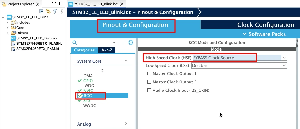
Before generating the project, we must configure the system clock. Open the Clock Configuration tab in CubeMX.
For the STM32F446RE, we will use the 8 MHz external crystal in bypass mode. This is the default clock source on the Nucleo board. The bypass mode uses the clock from the on-board ST-Link MCU.
We will feed this into the PLL and run the system at 180 MHz, which is the maximum frequency for this MCU.
The image below shows the complete PLL and clock configuration used to achieve 180 MHz.
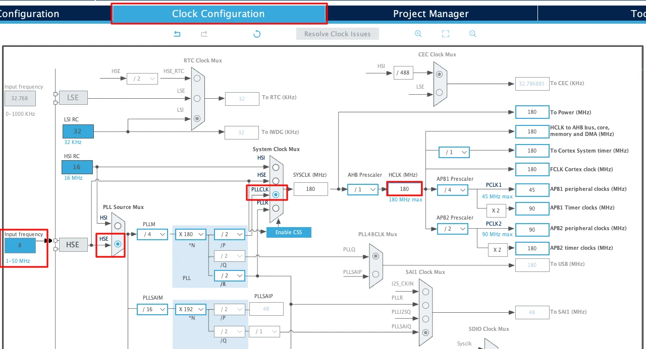
This fast system clock ensures accurate delays and smooth blinking using LL drivers. The SysTick timer will also run from this 180 MHz system clock, which becomes important in the delay functions we will use later.
Note for STM32F103C8
This MCU uses an 8 MHz external crystal as well, but its maximum frequency is 72 MHz. If you are using the Blue Pill, configure the PLL so that the final system clock is 72 MHz.
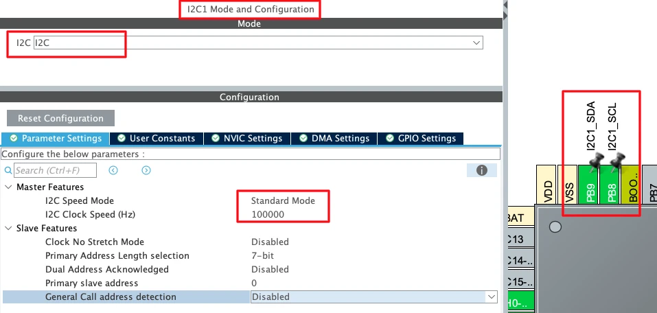
Configuring I2C1 Peripheral
I am going to use the I2C1 peripheral. Configure it in Standard Mode (100kHz), which is the most common I2C speed and works reliably with all devices.
The image below shows the I2C1 configuration in STM32CubeMX.
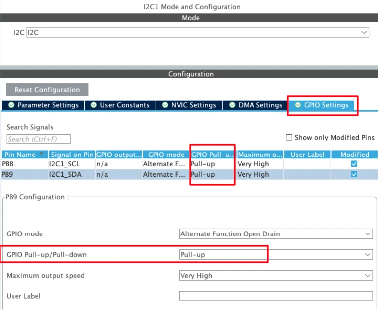
CubeMX automatically assigns the default I2C1 pins:
- PB6 → SCL (Clock Line)
- PB7 → SDA (Data Line)
These pins are standard for I2C1 on most STM32 boards. I have manually changes the pins to PB8 and PB9. These pins are easier to access on the nucleo boards.
Now configure the I2C parameters. Click on the Configuration tab under I2C1.
Set the following values:
- I2C Speed Mode: Standard Mode
- I2C Clock Speed: 100000 Hz (100 kHz)
Leave the rest of the settings at their default values.
STM32 microcontrollers support internal pull-up resistors on the I²C SCL and SDA lines. Enabling these pull-ups helps ensure proper bus idle levels when no external pull-up resistors or I²C devices are connected.
Enabling the LL Drivers
Before generating the code, we need to enable LL drivers instead of HAL. This ensures CubeMX generates lightweight LL functions for I2C and USART.
Open Project Manager → Advanced Settings. Enable LL Drivers for all peripherals. This ensures CubeMX generates clean, lightweight LL code.
The image below shows the LL driver selection in CubeMX.
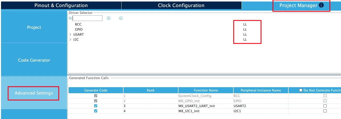
This step is critical. Without enabling LL drivers, CubeMX generates HAL code, which is heavier and not compatible with the LL functions.
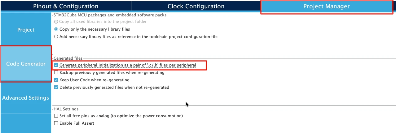
Next, go to Code Generator and select “Generate Peripheral Initialization as a pair of .c/.h files per peripheral”. This will generate a separate source files for all the peripherals we will use in a project.
Writing Single Byte to PCF8574 I/O Expander
The PCF8574 is one of the simplest I2C devices to work with. It provides 8 general-purpose I/O pins that we can control with a single byte. This makes it perfect for learning I2C write operations.
We will start by understanding how the PCF8574 works, then create a write function, and finally test it by controlling LEDs.
Understanding PCF8574 Operation
The PCF8574 is an 8-bit I/O expander. It has 8 pins (P0 to P7) that can work as inputs or outputs. We control all 8 pins by writing a single byte to the device.
How the PCF8574 Works:
The PCF8574 does not have internal registers. When you write a byte to it, that byte directly controls the output pins. Each bit in the byte corresponds to one pin:
- Bit 0 = P0
- Bit 1 = P1
- Bit 2 = P2
- …
- Bit 7 = P7
Writing 0xFF sets all pins HIGH. Writing 0x00 sets all pins LOW.
PCF8574 pinout:
The image below shows the available pins on the PCF8574 module.
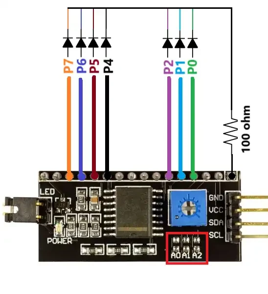
Common PCF8574 Addresses:
The PCF8574 comes in two variants with different address ranges:
- PCF8574: 0x20 to 0x27
- PCF8574A: 0x38 to 0x3F
The exact address depends on the A0, A1, and A2 pins on the module. Most modules use address 0x27 or 0x3F by default.
Creating the Single Byte Write Function
Now we create a function that writes a single byte to the PCF8574. This function follows the I2C write sequence we learned earlier.
void i2c_Write_byte(uint8_t slaveAddress, uint8_t data)
{
    // Generate START condition
    LL_I2C_GenerateStartCondition(I2C1);
    while(!LL_I2C_IsActiveFlag_SB(I2C1));

    // Send PCF8574 address with write bit
    LL_I2C_TransmitData8(I2C1, (slaveAddress << 1) | 0x00);
    while(!LL_I2C_IsActiveFlag_ADDR(I2C1));
    LL_I2C_ClearFlag_ADDR(I2C1);

    // Send data byte
    LL_I2C_TransmitData8(I2C1, data);
    while(!LL_I2C_IsActiveFlag_TXE(I2C1));

    // Generate STOP condition
    LL_I2C_GenerateStopCondition(I2C1);
}This function takes two parameters, the slave address of the device and the data byte to write.
How the Function Works:
- We generate the START condition and wait for the SB flag
- Then send the device address with the write bit (0)
- and wait for the ADDR flag and clear it
- Next, send the data byte
- and wait for the TXE flag (transmit buffer empty)
- Finally, generate the STOP condition
The entire transaction takes just a few microseconds. After the STOP condition, the PCF8574 immediately updates its output pins.
Testing PCF8574 LED Control
Now we test the function by controlling LEDs connected to the PCF8574. We will create a simple blinking pattern that cycles through different LED combinations.
The code below controls three LEDs connected to the PCF8574 module.
int main(void)
{
    // ... CubeMX generated initialization code ...
  while (1)
  {
    /* USER CODE BEGIN 3 */
	  i2c_Write_byte(0x27, 0x00);  // Turn OFF all LEDs (0b00000000)
	  LL_mDelay(500);
	  i2c_Write_byte(0x27, 0x01);  // Turn on LED 1 (0b00000001)
	  LL_mDelay(500);
	  i2c_Write_byte(0x27, 0x02);  // Turn on LED 2 (0b00000010)
	  LL_mDelay(500);
	  i2c_Write_byte(0x27, 0x04);  // Turn on LED 3 (0b00000100)
	  LL_mDelay(500);
	  i2c_Write_byte(0x27, 0xFF);  // Turn on all LEDs (0b11111111)
	  LL_mDelay(500);
  }
}Here we call the function i2c_Write_byte() to turn one LED ON at a time. The LEDs rotate every 500ms.
Output: Verifying LED Control
When we run this code, the LEDs connected to the PCF8574 will cycle through the programmed patterns. The gif below shows the LEDs blinking.
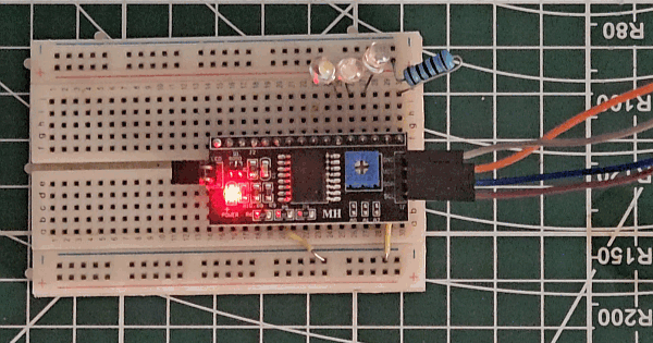
The PCF8574 responds instantly to write commands. There is no delay between sending the byte and seeing the LED change. This makes it perfect for real-time control applications.
Writing Multiple Bytes to AT24C EEPROM
EEPROM modules store data permanently, even when power is disconnected. Writing multiple bytes to EEPROM demonstrates how I2C handles sequential data transmission in a single transaction.
The AT24C EEPROM is perfect for this example because it requires memory addressing and shows how to write several bytes at once.
EEPROM Page Write Operation Explained
EEPROM devices use memory addresses to determine where data should be stored. When we write multiple bytes, the EEPROM automatically increments its internal address counter after each byte.
How Multi-Byte Write Works:
The write sequence includes the device address, memory address, and then all the data bytes. The EEPROM receives everything in one continuous transaction.
The image below shows the I2C multi-byte write sequence for EEPROM with memory address and multiple data bytes.

EEPROM Address Format:
AT24C EEPROMs use 16-bit addressing. We must send two bytes for the memory address:
- High byte: Upper 8 bits of the address
- Low byte: Lower 8 bits of the address
For address 0x0010:
- High byte = 0x00
- Low byte = 0x10
After we send the STOP condition, the EEPROM needs about 5ms to complete the internal write cycle. We must wait before performing another write operation.
Creating Multi-Byte Write Function
Now we create a function that writes multiple bytes to EEPROM. This function handles everything: device address, memory address, and data transmission.
void I2C_Mem_Write(uint8_t slaveAddress, uint16_t memAddress, uint8_t *data, uint16_t length)
{
    // Generate START condition
    LL_I2C_GenerateStartCondition(I2C1);
    while(!LL_I2C_IsActiveFlag_SB(I2C1));

    // Send device address with write bit
    LL_I2C_TransmitData8(I2C1, (slaveAddress << 1) | 0x00);
    while(!LL_I2C_IsActiveFlag_ADDR(I2C1));
    LL_I2C_ClearFlag_ADDR(I2C1);

    // Send memory address high byte
    LL_I2C_TransmitData8(I2C1, (uint8_t)(memAddress >> 8));
    while(!LL_I2C_IsActiveFlag_TXE(I2C1));

    // Send memory address low byte
    LL_I2C_TransmitData8(I2C1, (uint8_t)(memAddress & 0xFF));
    while(!LL_I2C_IsActiveFlag_TXE(I2C1));

    // Send all data bytes
    for(uint16_t i = 0; i < length; i++)
    {
        LL_I2C_TransmitData8(I2C1, data[i]);
        while(!LL_I2C_IsActiveFlag_TXE(I2C1));
    }

    // Generate STOP condition
    LL_I2C_GenerateStopCondition(I2C1);

    // Wait for EEPROM write cycle to complete
    LL_mDelay(5);
}This function takes four parameters:
slaveAddress: 7-bit I2C address of the EEPROM (typically 0x50)memAddress: 16-bit memory location where writing startsdata: Pointer to the data arraylength: Number of bytes to write
How the Function Works:
- Generate START and wait for SB flag to set
- Send device address with write bit
- Clear ADDR flag after acknowledgment
- Send high byte of memory address
- Send low byte of memory address
- Loop through the data array and send each byte
- Generate STOP condition
- Wait 5ms for internal write cycle
The 5ms delay is essential. The EEPROM cannot accept new commands while it writes data to its memory cells.
Complete Multi-Byte Write Example
Now we write a complete example that demonstrates writing a text string to EEPROM.
First, prepare the data outside the main function:
uint8_t message[] = "Hello STM32!";
uint16_t msg_length = sizeof(message) - 1; // Exclude null terminatorThen use it in the main function:
int main(void)
{
    // ... CubeMX generated initialization code ...

    /* USER CODE BEGIN 2 */

    I2C_Mem_Write(0x50, 0x0000, message, msg_length);

    /* USER CODE END 2 */

    while (1)
    {

    }
}This simple example writes “Hello STM32!” to EEPROM starting at address 0x0000. The function automatically handles sending all 12 bytes in one transaction.
Reading Back Data to Verify Write Operations
After writing data to EEPROM, we need to verify that the write was successful. Reading back the data confirms that our write function works correctly and the EEPROM stored the information properly.
This section shows a simple read function and how to use it to verify our previous writes. We keep this brief since the focus of this tutorial is on write operations.
Creating EEPROM Read Function
Reading from EEPROM requires a special sequence. We first write the memory address we want to read from, then generate a repeated START and read the data.
void I2C_Mem_Read(uint8_t slaveAddress, uint16_t memAddress, uint8_t *data, uint16_t length)
{
    // Generate START condition
    LL_I2C_GenerateStartCondition(I2C1);
    while(!LL_I2C_IsActiveFlag_SB(I2C1));

    // Send device address with write bit
    LL_I2C_TransmitData8(I2C1, (slaveAddress << 1) | 0x00);
    while(!LL_I2C_IsActiveFlag_ADDR(I2C1));
    LL_I2C_ClearFlag_ADDR(I2C1);

    // Send memory address high byte
    LL_I2C_TransmitData8(I2C1, (uint8_t)(memAddress >> 8));
    while(!LL_I2C_IsActiveFlag_TXE(I2C1));

    // Send memory address low byte
    LL_I2C_TransmitData8(I2C1, (uint8_t)(memAddress & 0xFF));
    while(!LL_I2C_IsActiveFlag_TXE(I2C1));

    // Generate repeated START condition
    LL_I2C_GenerateStartCondition(I2C1);
    while(!LL_I2C_IsActiveFlag_SB(I2C1));

    // Send device address with read bit
    LL_I2C_TransmitData8(I2C1, (slaveAddress << 1) | 0x01);
    while(!LL_I2C_IsActiveFlag_ADDR(I2C1));

    // Enable ACK for receiving data
    LL_I2C_AcknowledgeNextData(I2C1, LL_I2C_ACK);
    LL_I2C_ClearFlag_ADDR(I2C1);

    // Read all data bytes
    for(uint16_t i = 0; i < length; i++)
    {
        if(i == length - 1)
        {
            // Last byte: send NACK
            LL_I2C_AcknowledgeNextData(I2C1, LL_I2C_NACK);
        }

        while(!LL_I2C_IsActiveFlag_RXNE(I2C1));
        data[i] = LL_I2C_ReceiveData8(I2C1);
    }

    // Generate STOP condition
    LL_I2C_GenerateStopCondition(I2C1);
}This function sends the memory address, then switches to read mode and retrieves the requested number of bytes. The last byte receives a NACK to signal the end of the read operation.
We will cover I2C_Read() in depth in the next tutorial.
Verifying Written Data
Now we combine the write and read functions to verify data storage.
uint8_t message[] = "Hello STM32!";
uint16_t msg_length = sizeof(message) - 1;
uint8_t read_buffer[20];  // Buffer to store read data

int main(void)
{
    // ... CubeMX generated initialization code ...

    /* USER CODE BEGIN 2 */

    // Write data to EEPROM
    I2C_Mem_Write(0x50, 0x0000, message, msg_length);

    // Small delay after write
    LL_mDelay(10);

    // Read back the data
    I2C_Mem_Read(0x50, 0x0000, read_buffer, msg_length);

    /* USER CODE END 2 */

    while (1)
    {

    }
}This code writes the message to EEPROM, waits briefly, then reads it back into a buffer. The data in read_buffer should match the original message.
Conclusion
In this tutorial, we learned how to perform I2C write operations using STM32 Low-Layer (LL) drivers. We started by understanding the I2C write transaction sequence, including START conditions, address transmission, data bytes, and STOP conditions.
We implemented two practical examples. First, we controlled a PCF8574 I/O expander with single-byte writes to blink LEDs. This showed the simplest form of I2C communication. Then we wrote multiple bytes to AT24C EEPROM, which demonstrated memory addressing and sequential data transmission.
The tutorial covered creating reusable write functions that handle both single-byte and multi-byte operations. The write functions we created work with any I2C device, not just EEPROM and I/O expanders. You can adapt them for sensors, displays, RTCs, and other I2C peripherals. The core sequence remains the same: START, address, data, STOP.
Browse More STM32 LL Tutorials
STM32 UART using LL Drivers (Part 4): Receive Data in Interrupt Mode
STM32 UART using LL Drivers (Part 5): Receive Using DMA (Normal and Circular Mode)
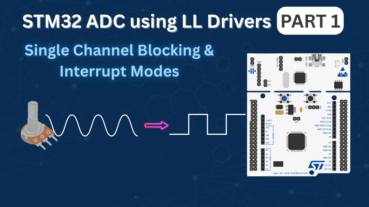
STM32 ADC Using LL Drivers (Part 1): Single Channel Blocking and Interrupt Mode
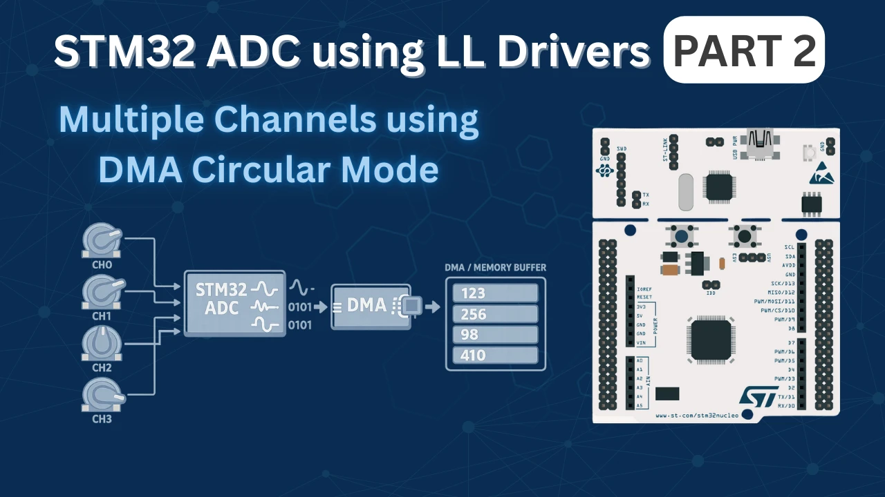
STM32 ADC Using LL Drivers (Part 2): Multiple Channels using DMA Mode
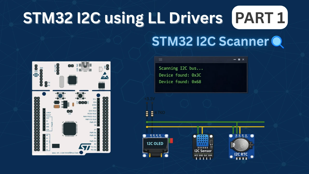
STM32 I2C using LL Drivers (Part 1): I2C Scanner to Detect I2C Devices with STM32CubeMX
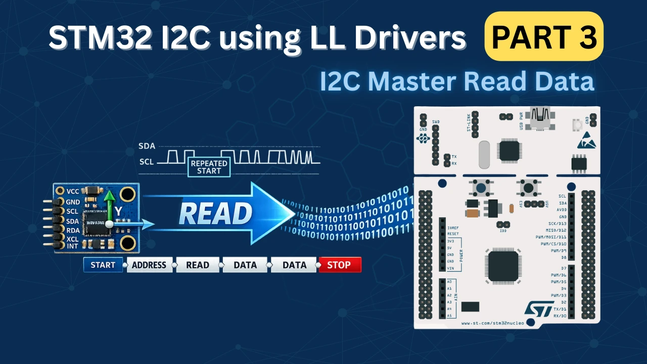
STM32 I2C Using LL Drivers (Part 3): Read Sensor Data from MPU6050
STM32 LL I2C Project Download

STM32 LL I2C FAQs

Subscribe
Login
0 Comments
Newest
